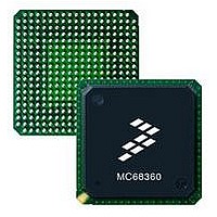
MC68EN360CAI25L Freescale Semiconductor, MC68EN360CAI25L Datasheet - Page 751

MC68EN360CAI25L
Manufacturer Part Number
MC68EN360CAI25L
Description
IC MPU QUICC 25MHZ 240-FQFP
Manufacturer
Freescale Semiconductor
Series
MC68000r
Datasheets
1.MC68EN302AG20BT.pdf
(8 pages)
2.MC68EN360VR25L.pdf
(14 pages)
3.MC68EN360VR25L.pdf
(2 pages)
4.MC68EN360CAI25L.pdf
(962 pages)
Specifications of MC68EN360CAI25L
Processor Type
M683xx 32-Bit
Speed
25MHz
Voltage
5V
Mounting Type
Surface Mount
Package / Case
240-FQFP
Core Size
32 Bit
Cpu Speed
25MHz
Embedded Interface Type
SCP, TDM
Digital Ic Case Style
FQFP
No. Of Pins
240
Supply Voltage Range
4.75V To 5.25V
Rohs Compliant
Yes
Family Name
M68xxx
Device Core
ColdFire
Device Core Size
32b
Frequency (max)
25MHz
Instruction Set Architecture
RISC
Supply Voltage 1 (typ)
5V
Operating Supply Voltage (max)
5.25V
Operating Supply Voltage (min)
4.75V
Operating Temp Range
-40C to 85C
Operating Temperature Classification
Industrial
Mounting
Surface Mount
Pin Count
240
Package Type
FQFP
Lead Free Status / RoHS Status
Lead free / RoHS Compliant
Features
-
Lead Free Status / Rohs Status
Compliant
Available stocks
Company
Part Number
Manufacturer
Quantity
Price
Company:
Part Number:
MC68EN360CAI25L
Manufacturer:
APLHA
Quantity:
12 000
Company:
Part Number:
MC68EN360CAI25L
Manufacturer:
Freescale Semiconductor
Quantity:
10 000
Part Number:
MC68EN360CAI25L
Manufacturer:
FREESCALE
Quantity:
20 000
- MC68EN302AG20BT PDF datasheet
- MC68EN360VR25L PDF datasheet #2
- MC68EN360VR25L PDF datasheet #3
- MC68EN360CAI25L PDF datasheet #4
- Current page: 751 of 962
- Download datasheet (4Mb)
the serial interface clock route register (SICR), and the serial interface command register
(SICMR).
9.4 USING THE QUICC MC68040 COMPANION MODE
The following paragraphs describe how to increase the performance of a QUICC-based sys-
tem by using an MC68EC040 to replace the CPU32+ core on the QUICC. When the
CPU32+ core on the QUICC is disabled, the QUICC is in slave mode. In slave mode,
another external processor may be used instead of the on-chip CPU32+ core. The QUICC,
however, has special features for providing a glueless interface to an external MC68EC040
(or other M68040 family member). This mode is called MC68040 companion mode.
The MS bits select the serial interface mode on the MC68302: NMSI, IDL, GCI, and PCM
highway. On the QUICC, the choice is simply to enable or disable the time slot assigner.
Once the time slot assigner is enabled, it may be programmed in the SI RAM to implement
IDL, GCI, PCM highway, and many other options. Additionally, on the QUICC, two TDM
interfaces are simultaneously available, not just one. Thus, on the QUICC, the MS bits ef-
fectively become the two enable bits, ENa and ENb, in the SIGMR.
The MSC2 and MSC3 bits are generalized on the QUICC to the SC bits in the SICR. On
the QUICC, one SC bit exists for each SCC.
The DRB and DRA bit functions are implemented by programming the QUICC SI RAM.
The B1RB and B1RA bit functions are implemented by programming the QUICC SI RAM.
The B2RB and B2RA bit functions are implemented by programming the QUICC SI RAM.
The SDC1 and SDC2 bit functions as well as many other options are implemented by pro-
gramming the QUICC SI RAM. Note that four strobe outputs are available on the QUICC,
not just two.
The two SDIAG bits are located in the QUICC SIMODE register and are renamed the
SDM bits. Furthermore, on the QUICC, two sets of SDM bits exist to support TDMa and
TDMb.
The SYNC bit function is implemented by programming the QUICC SI RAM.
The SCIT bit function is called the GM bit in the QUICC SIMODE register, and is available
on both TDMa and TDMb.
The SETZ bit function is called the STZ bit in the QUICC SIMODE register, and is avail-
able on both TDMa and TDMb.
The QUICC does not require the use of the L1SY0 and L1SY1
pins to synchronize the SCC to a given time slot. This is now
handled by the time slot assigner using an external frame sync.
Thus, the QUICC contains other programming options to specify
the desired behavior of the frame sync and the associated exter-
nal clocks. Examples are the FE, CE, CRT, DSC, and FSD bits
in SIMODE.
Freescale Semiconductor, Inc.
For More Information On This Product,
MC68360 USER’S MANUAL
Go to: www.freescale.com
NOTE
Applications
Related parts for MC68EN360CAI25L
Image
Part Number
Description
Manufacturer
Datasheet
Request
R
Part Number:
Description:
Manufacturer:
Freescale Semiconductor, Inc
Datasheet:
Part Number:
Description:
Manufacturer:
Freescale Semiconductor, Inc
Datasheet:
Part Number:
Description:
Manufacturer:
Freescale Semiconductor, Inc
Datasheet:
Part Number:
Description:
Manufacturer:
Freescale Semiconductor, Inc
Datasheet:
Part Number:
Description:
Manufacturer:
Freescale Semiconductor, Inc
Datasheet:
Part Number:
Description:
Manufacturer:
Freescale Semiconductor, Inc
Datasheet:
Part Number:
Description:
Manufacturer:
Freescale Semiconductor, Inc
Datasheet:
Part Number:
Description:
Manufacturer:
Freescale Semiconductor, Inc
Datasheet:
Part Number:
Description:
Manufacturer:
Freescale Semiconductor, Inc
Datasheet:
Part Number:
Description:
Manufacturer:
Freescale Semiconductor, Inc
Datasheet:
Part Number:
Description:
Manufacturer:
Freescale Semiconductor, Inc
Datasheet:
Part Number:
Description:
Manufacturer:
Freescale Semiconductor, Inc
Datasheet:
Part Number:
Description:
Manufacturer:
Freescale Semiconductor, Inc
Datasheet:
Part Number:
Description:
Manufacturer:
Freescale Semiconductor, Inc
Datasheet:
Part Number:
Description:
Manufacturer:
Freescale Semiconductor, Inc
Datasheet:


