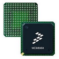
MC68EN360CAI25L Freescale Semiconductor, MC68EN360CAI25L Datasheet - Page 63

MC68EN360CAI25L
Manufacturer Part Number
MC68EN360CAI25L
Description
IC MPU QUICC 25MHZ 240-FQFP
Manufacturer
Freescale Semiconductor
Series
MC68000r
Datasheets
1.MC68EN302AG20BT.pdf
(8 pages)
2.MC68EN360VR25L.pdf
(14 pages)
3.MC68EN360VR25L.pdf
(2 pages)
4.MC68EN360CAI25L.pdf
(962 pages)
Specifications of MC68EN360CAI25L
Processor Type
M683xx 32-Bit
Speed
25MHz
Voltage
5V
Mounting Type
Surface Mount
Package / Case
240-FQFP
Core Size
32 Bit
Cpu Speed
25MHz
Embedded Interface Type
SCP, TDM
Digital Ic Case Style
FQFP
No. Of Pins
240
Supply Voltage Range
4.75V To 5.25V
Rohs Compliant
Yes
Family Name
M68xxx
Device Core
ColdFire
Device Core Size
32b
Frequency (max)
25MHz
Instruction Set Architecture
RISC
Supply Voltage 1 (typ)
5V
Operating Supply Voltage (max)
5.25V
Operating Supply Voltage (min)
4.75V
Operating Temp Range
-40C to 85C
Operating Temperature Classification
Industrial
Mounting
Surface Mount
Pin Count
240
Package Type
FQFP
Lead Free Status / RoHS Status
Lead free / RoHS Compliant
Features
-
Lead Free Status / Rohs Status
Compliant
Available stocks
Company
Part Number
Manufacturer
Quantity
Price
Company:
Part Number:
MC68EN360CAI25L
Manufacturer:
APLHA
Quantity:
12 000
Company:
Part Number:
MC68EN360CAI25L
Manufacturer:
Freescale Semiconductor
Quantity:
10 000
Part Number:
MC68EN360CAI25L
Manufacturer:
FREESCALE
Quantity:
20 000
- MC68EN302AG20BT PDF datasheet
- MC68EN360VR25L PDF datasheet #2
- MC68EN360VR25L PDF datasheet #3
- MC68EN360CAI25L PDF datasheet #4
- Current page: 63 of 962
- Download datasheet (4Mb)
2.3 ON-CHIP PERIPHERALS SIGNAL INDEX
The input and output system signals for the QUICC peripherals are listed in Table 2-8. The
signal name, mnemonic, and a brief functional description are presented. For more detail on
each signal, refer to the specific module section. The peripherals pins are divided into three
ports: A, B, and C.
Port A has 16 pins, port B has 18 pins, and port C has 12 pins. All the following signals are
multiplexed with either port A, B, or C. All pins may be inputs or outputs; in addition, some
pins may be configured to be open-drain. See 7.14 Parallel I/O Ports for further details.
TIMER
Group
Master Mode
AVEC/IACK5
IDMA
SCC
Mnemonic
RAS1DD
IPIPE1/
PRTY0
PRTY1
PRTY2
DMA Acknowledge
Request to Send
Receive Reject
Transmit Data
Carrier Detect
DMA Request
Clear to Send
Signal Name
Receive Data
Receive Start
Timer Gate
Timer Input
DMA Done
Table 2-7. System Bus Signal Index (Slave Mode) (Continued)
Clocks
Row Address Select 1
Parity 0/Interrupt Out-
Parity 1/Interrupt Out-
Interrupt Output 0/
Autovector Output
Bus Clear Input/
Request Output
Signal Name
Double-Drive
Slave Mode
Parity 2/
put 2
put 1
Freescale Semiconductor, Inc.
TGATE2–TGATE1 An input to a timer that enables/disables the counting function. (I)
DREQ2–DREQ1 A request (input) to an IDMA channel to start an IDMA transfer. (I)
DONE2–DONE1 A bidirectional signal that indicates the last IDMA transfer in a block
DACK2–DACK1
For More Information On This Product,
Table 2-8. Peripherals Signal Index
RXD4–RXD1
TXD4–TXD1
RTS4–RTS1
CTS4–CTS1
CLK8–CLK1
Mnemonic
TIN4–TIN1
CD4–CD1
RSTRT1
RRJCT1
PRTY2/IOUT0/
PRTY0/IOUT2 Parity signals for D31–D24 writes/reads from/to external mem-
PRTY1/IOUT1 Parity signals for D23–D16 writes/reads from/to external mem-
Slave Mode
Mnemonic
MC68360 USER’S MANUAL
RAS1DD
Go to: www.freescale.com
RQOUT
AVECO
BCLRI/
Serial receive data input to the SCCs. (I)
Serial transmit data output from the SCCs. (O)
Request to send outputs indicate that the SCC is ready to transmit
data. (O)
Clear to send inputs indicate to the SCC that data transmission may
begin. (I)
Carrier detect inputs indicate that the SCC should begin reception of
data. (I)
This output from SCC1 identifies the start of a receive frame. Can be
used by an Ethernet CAM to perform address matching. (O)
This input to SCC1 allows a CAM to reject the current Ethernet frame
after it determines the frame address did not match. (I)
Input clocks to the SCCs, SMCs, SI, and the baud rate generators. (I)
An acknowledgement (output) by the IDMA that an IDMA transfer is
in progress. (O)
of data. (I/O)
Time reference input to the timer that allows it to function as a
counter. (I)
ory bank (I/O), or interrupt output 2 signal (O).
ory bank (I/O) or interrupt output 1 signal. (O)
Parity signals for D15–D8 writes/reads from/to external memory
bank (I/O), or interrupt output 0 signal (O), or RQOUT as a sin-
gle interrupt request output (O).
Signal output to the external processor to generate an internal
vector number during an interrupt acknowledge cycle. (three-
stated O)
Signals that an external device requests the QUICC to release
the external bus (I), or row address select 1 double-drive (O).
Slave Mode Function
Function
Signal Descriptions
Related parts for MC68EN360CAI25L
Image
Part Number
Description
Manufacturer
Datasheet
Request
R
Part Number:
Description:
Manufacturer:
Freescale Semiconductor, Inc
Datasheet:
Part Number:
Description:
Manufacturer:
Freescale Semiconductor, Inc
Datasheet:
Part Number:
Description:
Manufacturer:
Freescale Semiconductor, Inc
Datasheet:
Part Number:
Description:
Manufacturer:
Freescale Semiconductor, Inc
Datasheet:
Part Number:
Description:
Manufacturer:
Freescale Semiconductor, Inc
Datasheet:
Part Number:
Description:
Manufacturer:
Freescale Semiconductor, Inc
Datasheet:
Part Number:
Description:
Manufacturer:
Freescale Semiconductor, Inc
Datasheet:
Part Number:
Description:
Manufacturer:
Freescale Semiconductor, Inc
Datasheet:
Part Number:
Description:
Manufacturer:
Freescale Semiconductor, Inc
Datasheet:
Part Number:
Description:
Manufacturer:
Freescale Semiconductor, Inc
Datasheet:
Part Number:
Description:
Manufacturer:
Freescale Semiconductor, Inc
Datasheet:
Part Number:
Description:
Manufacturer:
Freescale Semiconductor, Inc
Datasheet:
Part Number:
Description:
Manufacturer:
Freescale Semiconductor, Inc
Datasheet:
Part Number:
Description:
Manufacturer:
Freescale Semiconductor, Inc
Datasheet:
Part Number:
Description:
Manufacturer:
Freescale Semiconductor, Inc
Datasheet:


