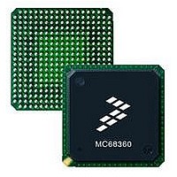
MC68EN360CAI25L Freescale Semiconductor, MC68EN360CAI25L Datasheet - Page 786

MC68EN360CAI25L
Manufacturer Part Number
MC68EN360CAI25L
Description
IC MPU QUICC 25MHZ 240-FQFP
Manufacturer
Freescale Semiconductor
Series
MC68000r
Datasheets
1.MC68EN302AG20BT.pdf
(8 pages)
2.MC68EN360VR25L.pdf
(14 pages)
3.MC68EN360VR25L.pdf
(2 pages)
4.MC68EN360CAI25L.pdf
(962 pages)
Specifications of MC68EN360CAI25L
Processor Type
M683xx 32-Bit
Speed
25MHz
Voltage
5V
Mounting Type
Surface Mount
Package / Case
240-FQFP
Core Size
32 Bit
Cpu Speed
25MHz
Embedded Interface Type
SCP, TDM
Digital Ic Case Style
FQFP
No. Of Pins
240
Supply Voltage Range
4.75V To 5.25V
Rohs Compliant
Yes
Family Name
M68xxx
Device Core
ColdFire
Device Core Size
32b
Frequency (max)
25MHz
Instruction Set Architecture
RISC
Supply Voltage 1 (typ)
5V
Operating Supply Voltage (max)
5.25V
Operating Supply Voltage (min)
4.75V
Operating Temp Range
-40C to 85C
Operating Temperature Classification
Industrial
Mounting
Surface Mount
Pin Count
240
Package Type
FQFP
Lead Free Status / RoHS Status
Lead free / RoHS Compliant
Features
-
Lead Free Status / Rohs Status
Compliant
Available stocks
Company
Part Number
Manufacturer
Quantity
Price
Company:
Part Number:
MC68EN360CAI25L
Manufacturer:
APLHA
Quantity:
12 000
Company:
Part Number:
MC68EN360CAI25L
Manufacturer:
Freescale Semiconductor
Quantity:
10 000
Part Number:
MC68EN360CAI25L
Manufacturer:
FREESCALE
Quantity:
20 000
- MC68EN302AG20BT PDF datasheet
- MC68EN360VR25L PDF datasheet #2
- MC68EN360VR25L PDF datasheet #3
- MC68EN360CAI25L PDF datasheet #4
- Current page: 786 of 962
- Download datasheet (4Mb)
Applications
9.6.7.2 CONFIGURING THE MEMORY CONTROLLER. The
describe configuring the memory controller.
For information on configuring the global memory register (GMR), refer to 9.1 Minimum Sys-
tem Configuration.
The memory controller status register (MSTAT) is used for reporting parity errors and does
not require initialization.
Eight base registers (BRs) exist, one for each memory bank. BR6 and BR7 for CS6 and CS7
will be specified with the 53C90 address being $04001000. Please refer to 9.1 Minimum
System Configuration for DRAM and other memory configurations.
Eight option registers (ORs) exist, one for each memory bank. The following information is
valid for registers OR6 and OR7:
Therefore, OR7 = $2FFFF804 and OR6 = $1FFFF804.
9.7 USING THE QUICC AS A TAP CONTROLLER FOR BOARD SELF-TEST
An assembled board is often tested with complex test equipment using a unique test port or
a bed-of-nails fixture. This procedure becomes more difficult as device packages and fea-
tures become smaller. The objective of the JTAG standard is to define a boundary scan
architecture that can be adopted as a part of an integrated circuit to perform both an in-circuit
test and a verification of the interconnection between different devices.
The JTAG standard defines test logic that can be integrated into a device to perform:
9-66
BR7 = $0400104D. Address decoded is $04001xxx, function codes are xxxx (don't care,
will be masked in OR7), TRLXQ and CSNTQ are set, parity is enabled, read and write ac-
cesses are allowed, and this base register is valid.
BR6 = $04001805. Same as BR7, except TRLXQ and CSNTQ are not set and the next
consecutive 2K memory block is selected.
DSSEL should be 0.
SPS1–SPS0 should be 10 (indicating port size is 8 bits).
PGME should be 0 since this is not DRAM.
BCYC1–BCYC0 are not used and should be cleared.
FCM3–FCM0 may be cleared to zeros to allow the chip select or RAS line to assert on all
function codes, except CPU space (interrupt acknowledge). It is advisable to program
FCM3–FCM0 to zeros, at least during the initial stages of debugging.
The AM27–AM11 bits will mask the address if they are cleared. In this application, they
are all set to allow decoding.
The TCYC bits should be set to determine the number of wait states required—one wait
state on CS7 (0010) and no wait states on CS6 (0001).
1. Testing of the interconnection between devices once they have been mounted on a
printed circuit board or any other substrate.
Freescale Semiconductor, Inc.
For More Information On This Product,
MC68360 USER’S MANUAL
Go to: www.freescale.com
following
paragraphs
Related parts for MC68EN360CAI25L
Image
Part Number
Description
Manufacturer
Datasheet
Request
R
Part Number:
Description:
Manufacturer:
Freescale Semiconductor, Inc
Datasheet:
Part Number:
Description:
Manufacturer:
Freescale Semiconductor, Inc
Datasheet:
Part Number:
Description:
Manufacturer:
Freescale Semiconductor, Inc
Datasheet:
Part Number:
Description:
Manufacturer:
Freescale Semiconductor, Inc
Datasheet:
Part Number:
Description:
Manufacturer:
Freescale Semiconductor, Inc
Datasheet:
Part Number:
Description:
Manufacturer:
Freescale Semiconductor, Inc
Datasheet:
Part Number:
Description:
Manufacturer:
Freescale Semiconductor, Inc
Datasheet:
Part Number:
Description:
Manufacturer:
Freescale Semiconductor, Inc
Datasheet:
Part Number:
Description:
Manufacturer:
Freescale Semiconductor, Inc
Datasheet:
Part Number:
Description:
Manufacturer:
Freescale Semiconductor, Inc
Datasheet:
Part Number:
Description:
Manufacturer:
Freescale Semiconductor, Inc
Datasheet:
Part Number:
Description:
Manufacturer:
Freescale Semiconductor, Inc
Datasheet:
Part Number:
Description:
Manufacturer:
Freescale Semiconductor, Inc
Datasheet:
Part Number:
Description:
Manufacturer:
Freescale Semiconductor, Inc
Datasheet:
Part Number:
Description:
Manufacturer:
Freescale Semiconductor, Inc
Datasheet:


