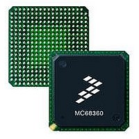
MC68EN360CAI25L Freescale Semiconductor, MC68EN360CAI25L Datasheet - Page 569

MC68EN360CAI25L
Manufacturer Part Number
MC68EN360CAI25L
Description
IC MPU QUICC 25MHZ 240-FQFP
Manufacturer
Freescale Semiconductor
Series
MC68000r
Datasheets
1.MC68EN302AG20BT.pdf
(8 pages)
2.MC68EN360VR25L.pdf
(14 pages)
3.MC68EN360VR25L.pdf
(2 pages)
4.MC68EN360CAI25L.pdf
(962 pages)
Specifications of MC68EN360CAI25L
Processor Type
M683xx 32-Bit
Speed
25MHz
Voltage
5V
Mounting Type
Surface Mount
Package / Case
240-FQFP
Core Size
32 Bit
Cpu Speed
25MHz
Embedded Interface Type
SCP, TDM
Digital Ic Case Style
FQFP
No. Of Pins
240
Supply Voltage Range
4.75V To 5.25V
Rohs Compliant
Yes
Family Name
M68xxx
Device Core
ColdFire
Device Core Size
32b
Frequency (max)
25MHz
Instruction Set Architecture
RISC
Supply Voltage 1 (typ)
5V
Operating Supply Voltage (max)
5.25V
Operating Supply Voltage (min)
4.75V
Operating Temp Range
-40C to 85C
Operating Temperature Classification
Industrial
Mounting
Surface Mount
Pin Count
240
Package Type
FQFP
Lead Free Status / RoHS Status
Lead free / RoHS Compliant
Features
-
Lead Free Status / Rohs Status
Compliant
Available stocks
Company
Part Number
Manufacturer
Quantity
Price
Company:
Part Number:
MC68EN360CAI25L
Manufacturer:
APLHA
Quantity:
12 000
Company:
Part Number:
MC68EN360CAI25L
Manufacturer:
Freescale Semiconductor
Quantity:
10 000
Part Number:
MC68EN360CAI25L
Manufacturer:
FREESCALE
Quantity:
20 000
- MC68EN302AG20BT PDF datasheet
- MC68EN360VR25L PDF datasheet #2
- MC68EN360VR25L PDF datasheet #3
- MC68EN360CAI25L PDF datasheet #4
- Current page: 569 of 962
- Download datasheet (4Mb)
Additionally, the CAM control logic may wish to provide additional information on the PB15–
PB8 pins. The QUICC Ethernet controller will write this additional byte to memory during the
last SDMA write if the SIP bit is set in the PSMR. This information tag is sampled by the
QUICC Ethernet controller as the last FCS byte is read from the receive FIFO. The informa-
tion TAG should be provided by the CAM control logic no later than when RENA is negated
at the end of a non-collision frame, and should be held stable on the PB15–PB8 pins until
the SDACK2–SDACK1 pins signal that the tag byte is being written to memory.
The parallel interface option is shown in Figure 7-69. The QUICC outputs two signals every
time it writes Ethernet frame data to system memory. The signals SDMA acknowledge
(SDACK2–SDACK1), are asserted during all bus cycles on which Ethernet frame data is
written to memory. (These signals are not used for other protocols.)
The CAM control logic uses these pins to enable the CAM writes simultaneously with system
memory writes. In this way, the CAM captures the frame data at the same time that it is being
written to system memory. The chief advantage of this approach is that the data is already
in parallel form when it leaves the QUICC.
The SDACK2–SDACK1 signals are asserted during all bus cycles writes of the frame data.
A certain SDACK2–SDACK1 combination specifically identifies the first 32-bits of the frame,
another identifies all mid-frame data, and a third combination identifies the last 32-bit bus
write of the frame (only if the tag byte is appended). The tag byte is appended from the sam-
ple of PB15–PB8 if the SIP bit is set in the PSMR. The tag byte will always be in byte 3 of
the last 32-bit write. The Rx BD Data Length does not include tag byte in the length calcu-
lation.
If the system memory is 32 bits, then the QUICC 32-bit write will take one bus cycle. If the
system memory is 16 bits or 8 bits, then the QUICC 32-bit write will take two or four bus
cycles. In any case, the SDACK2–SDACK1 signals are valid on each bus cycle of a 32-bit
write cycle and only during bus cycles associated with the Ethernet receiver.
Additionally, the user may choose a unique function code (FC3–FC0) associated with the
SDMA receive channel associated with the Ethernet SCC to have an alternate method of
identifying accesses from this SCC.
The tag byte is always written to byte 3 of the last SDMA write to
the buffer, and is not necessarily appended to the last byte of the
frame. The Rx BD Data Length does not show the length of the
tag byte in the frame. Also the SDACK2-1 signals will equal "00"
whenever the frame length is not an even multiple of 4 (i.e., it
does not depend on whether the tag byte is appended).
Freescale Semiconductor, Inc.
For More Information On This Product,
MC68360 USER’S MANUAL
Go to: www.freescale.com
NOTE
Serial Communication Controllers (SCCs)
Related parts for MC68EN360CAI25L
Image
Part Number
Description
Manufacturer
Datasheet
Request
R
Part Number:
Description:
Manufacturer:
Freescale Semiconductor, Inc
Datasheet:
Part Number:
Description:
Manufacturer:
Freescale Semiconductor, Inc
Datasheet:
Part Number:
Description:
Manufacturer:
Freescale Semiconductor, Inc
Datasheet:
Part Number:
Description:
Manufacturer:
Freescale Semiconductor, Inc
Datasheet:
Part Number:
Description:
Manufacturer:
Freescale Semiconductor, Inc
Datasheet:
Part Number:
Description:
Manufacturer:
Freescale Semiconductor, Inc
Datasheet:
Part Number:
Description:
Manufacturer:
Freescale Semiconductor, Inc
Datasheet:
Part Number:
Description:
Manufacturer:
Freescale Semiconductor, Inc
Datasheet:
Part Number:
Description:
Manufacturer:
Freescale Semiconductor, Inc
Datasheet:
Part Number:
Description:
Manufacturer:
Freescale Semiconductor, Inc
Datasheet:
Part Number:
Description:
Manufacturer:
Freescale Semiconductor, Inc
Datasheet:
Part Number:
Description:
Manufacturer:
Freescale Semiconductor, Inc
Datasheet:
Part Number:
Description:
Manufacturer:
Freescale Semiconductor, Inc
Datasheet:
Part Number:
Description:
Manufacturer:
Freescale Semiconductor, Inc
Datasheet:
Part Number:
Description:
Manufacturer:
Freescale Semiconductor, Inc
Datasheet:


