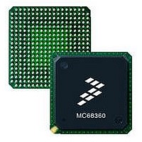
MC68EN360CAI25L Freescale Semiconductor, MC68EN360CAI25L Datasheet - Page 516

MC68EN360CAI25L
Manufacturer Part Number
MC68EN360CAI25L
Description
IC MPU QUICC 25MHZ 240-FQFP
Manufacturer
Freescale Semiconductor
Series
MC68000r
Datasheets
1.MC68EN302AG20BT.pdf
(8 pages)
2.MC68EN360VR25L.pdf
(14 pages)
3.MC68EN360VR25L.pdf
(2 pages)
4.MC68EN360CAI25L.pdf
(962 pages)
Specifications of MC68EN360CAI25L
Processor Type
M683xx 32-Bit
Speed
25MHz
Voltage
5V
Mounting Type
Surface Mount
Package / Case
240-FQFP
Core Size
32 Bit
Cpu Speed
25MHz
Embedded Interface Type
SCP, TDM
Digital Ic Case Style
FQFP
No. Of Pins
240
Supply Voltage Range
4.75V To 5.25V
Rohs Compliant
Yes
Family Name
M68xxx
Device Core
ColdFire
Device Core Size
32b
Frequency (max)
25MHz
Instruction Set Architecture
RISC
Supply Voltage 1 (typ)
5V
Operating Supply Voltage (max)
5.25V
Operating Supply Voltage (min)
4.75V
Operating Temp Range
-40C to 85C
Operating Temperature Classification
Industrial
Mounting
Surface Mount
Pin Count
240
Package Type
FQFP
Lead Free Status / RoHS Status
Lead free / RoHS Compliant
Features
-
Lead Free Status / Rohs Status
Compliant
Available stocks
Company
Part Number
Manufacturer
Quantity
Price
Company:
Part Number:
MC68EN360CAI25L
Manufacturer:
APLHA
Quantity:
12 000
Company:
Part Number:
MC68EN360CAI25L
Manufacturer:
Freescale Semiconductor
Quantity:
10 000
Part Number:
MC68EN360CAI25L
Manufacturer:
FREESCALE
Quantity:
20 000
- MC68EN302AG20BT PDF datasheet
- MC68EN360VR25L PDF datasheet #2
- MC68EN360VR25L PDF datasheet #3
- MC68EN360CAI25L PDF datasheet #4
- Current page: 516 of 962
- Download datasheet (4Mb)
Serial Communication Controllers (SCCs)
7.10.18.1 HDLC BUS KEY FEATURES. The HDLC bus controller contains the following
key features:
7.10.18.2 HDLC BUS OPERATION. The following paragraphs detail the operation of the
HDLC bus Controller.
7.10.18.2.1 Accessing the HDLC Bus. HDLC bus ensures an orderly access to the bus
when two or more transmitters attempt to access the bus simultaneously. In such a case,
one transmitter will always be successful in completing its transmission. This procedure
relies upon the use of HDLC flags consisting of the binary pattern 01111110 ($7E) and the
use of the zero bit insertion to prevent flag imitation.
While in the active condition (desiring to transmit), the HDLC bus controller will monitor the
bus through the CTS pin. It counts the number of one bits using the CTS pin, and if a zero
is detected, the internal counter is cleared.
Once 8 consecutive ones have been received, the HDLC bus controller will begin transmis-
sion on the line. While it is transmitting information on the bus, the transmitted data is con-
tinuously compared with the data actually on the bus. The CTS pin is used to sample the
external bus.
Figure 7-56 shows how the CTS pin is used. The CTS sample is taken halfway through the
bit time, using the rising edge of the transmit clock. If the transmitted bit is the same as the
received CTS sample, the HDLC bus controller continues its transmission. If, however, the
received CTS bit is zero, but the transmitted bit was 1, the HDLC controller ceases trans-
mission following that bit and returns to the active condition. Since the HDLC bus uses a
wired-OR scheme, a transmitted zero has priority over a transmitted one.
If the source address is included in the HDLC frame in addition to the destination address,
a predefined priority of nodes will result. In addition, the inclusion of a source address will
allow collisions to be detected no later than the end of the source address.
7-192
• Superset of the HDLC Controller Features
• Automatic HDLC Bus Access
• Automatic Retransmission in Case of a Collision
• May Be Used with the NMSI Mode or a TDM Bus
• Delayed RTS Mode
HDLC bus can be used with many different HDLC-based frame
formats. HDLC bus does not specify the type of HDLC protocol
used.
Freescale Semiconductor, Inc.
For More Information On This Product,
MC68360 USER’S MANUAL
Go to: www.freescale.com
NOTE
Related parts for MC68EN360CAI25L
Image
Part Number
Description
Manufacturer
Datasheet
Request
R
Part Number:
Description:
Manufacturer:
Freescale Semiconductor, Inc
Datasheet:
Part Number:
Description:
Manufacturer:
Freescale Semiconductor, Inc
Datasheet:
Part Number:
Description:
Manufacturer:
Freescale Semiconductor, Inc
Datasheet:
Part Number:
Description:
Manufacturer:
Freescale Semiconductor, Inc
Datasheet:
Part Number:
Description:
Manufacturer:
Freescale Semiconductor, Inc
Datasheet:
Part Number:
Description:
Manufacturer:
Freescale Semiconductor, Inc
Datasheet:
Part Number:
Description:
Manufacturer:
Freescale Semiconductor, Inc
Datasheet:
Part Number:
Description:
Manufacturer:
Freescale Semiconductor, Inc
Datasheet:
Part Number:
Description:
Manufacturer:
Freescale Semiconductor, Inc
Datasheet:
Part Number:
Description:
Manufacturer:
Freescale Semiconductor, Inc
Datasheet:
Part Number:
Description:
Manufacturer:
Freescale Semiconductor, Inc
Datasheet:
Part Number:
Description:
Manufacturer:
Freescale Semiconductor, Inc
Datasheet:
Part Number:
Description:
Manufacturer:
Freescale Semiconductor, Inc
Datasheet:
Part Number:
Description:
Manufacturer:
Freescale Semiconductor, Inc
Datasheet:
Part Number:
Description:
Manufacturer:
Freescale Semiconductor, Inc
Datasheet:


