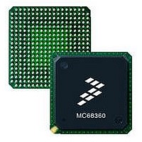
MC68EN360CAI25L Freescale Semiconductor, MC68EN360CAI25L Datasheet - Page 793

MC68EN360CAI25L
Manufacturer Part Number
MC68EN360CAI25L
Description
IC MPU QUICC 25MHZ 240-FQFP
Manufacturer
Freescale Semiconductor
Series
MC68000r
Datasheets
1.MC68EN302AG20BT.pdf
(8 pages)
2.MC68EN360VR25L.pdf
(14 pages)
3.MC68EN360VR25L.pdf
(2 pages)
4.MC68EN360CAI25L.pdf
(962 pages)
Specifications of MC68EN360CAI25L
Processor Type
M683xx 32-Bit
Speed
25MHz
Voltage
5V
Mounting Type
Surface Mount
Package / Case
240-FQFP
Core Size
32 Bit
Cpu Speed
25MHz
Embedded Interface Type
SCP, TDM
Digital Ic Case Style
FQFP
No. Of Pins
240
Supply Voltage Range
4.75V To 5.25V
Rohs Compliant
Yes
Family Name
M68xxx
Device Core
ColdFire
Device Core Size
32b
Frequency (max)
25MHz
Instruction Set Architecture
RISC
Supply Voltage 1 (typ)
5V
Operating Supply Voltage (max)
5.25V
Operating Supply Voltage (min)
4.75V
Operating Temp Range
-40C to 85C
Operating Temperature Classification
Industrial
Mounting
Surface Mount
Pin Count
240
Package Type
FQFP
Lead Free Status / RoHS Status
Lead free / RoHS Compliant
Features
-
Lead Free Status / Rohs Status
Compliant
Available stocks
Company
Part Number
Manufacturer
Quantity
Price
Company:
Part Number:
MC68EN360CAI25L
Manufacturer:
APLHA
Quantity:
12 000
Company:
Part Number:
MC68EN360CAI25L
Manufacturer:
Freescale Semiconductor
Quantity:
10 000
Part Number:
MC68EN360CAI25L
Manufacturer:
FREESCALE
Quantity:
20 000
- MC68EN302AG20BT PDF datasheet
- MC68EN360VR25L PDF datasheet #2
- MC68EN360VR25L PDF datasheet #3
- MC68EN360CAI25L PDF datasheet #4
- Current page: 793 of 962
- Download datasheet (4Mb)
Applications
The bit-banging pattern is created by writing and reading the array rows to the port as fast
as the CPU allows. The instructions to implement the shaded part of Figure 9-26 (indicated
by "repeat") are listed below. They are needed to perform one test clock cycle along with the
data signals. Assuming the output array address is located in address register A0, the input
array address is in address register A2, with the I/O port located at address A1 and the
length of the pattern in D0, one repeat cycle is as follows:
9-73
ROW NR
NOTES:
TMS
TDO
TCK
1. TCK rise and fall time
2. TMS, TDI data hold time
3. TMS, TDI data setup time
4. TCK to TDO valid
5. TCK cycle time
6. TCK pulse width
TDI
10
1
2
3
4
8
9
5
7
6
Figure 9-26. Bit Banging of Boundary Scan Pattern
M
T
S
0
0
0
0
0
0
1
1
0
0
6
1
1
D
0
0
0
T
0
0
0
0
0
I
Freescale Semiconductor, Inc.
For More Information On This Product,
5
0
1
0
T
C
K
1
1
0
1
1
0
0
4
MC68360 USER’S MANUAL
1
T
D
O
0
0
1
1
1
0
0
1
1
Go to: www.freescale.com
6
3
WRITE ROW NR 1
WRITE ROW NR 3
WRITE ROW NR 5
WRITE ROW NR 8
WRITE ROW NR 9
WRITE ROW NR 10
WRITE ROW NR 2
WRITE ROW NR 4
WRITE ROW NR 6
WRITE ROW NR 7
READ ROW NR 3
READ ROW NR 5
READ ROW NR 9
READ ROW NR 7
2
V
V
IH
IL
1
REPEAT
STABLE INPUT
OUTPUT VALID
Related parts for MC68EN360CAI25L
Image
Part Number
Description
Manufacturer
Datasheet
Request
R
Part Number:
Description:
Manufacturer:
Freescale Semiconductor, Inc
Datasheet:
Part Number:
Description:
Manufacturer:
Freescale Semiconductor, Inc
Datasheet:
Part Number:
Description:
Manufacturer:
Freescale Semiconductor, Inc
Datasheet:
Part Number:
Description:
Manufacturer:
Freescale Semiconductor, Inc
Datasheet:
Part Number:
Description:
Manufacturer:
Freescale Semiconductor, Inc
Datasheet:
Part Number:
Description:
Manufacturer:
Freescale Semiconductor, Inc
Datasheet:
Part Number:
Description:
Manufacturer:
Freescale Semiconductor, Inc
Datasheet:
Part Number:
Description:
Manufacturer:
Freescale Semiconductor, Inc
Datasheet:
Part Number:
Description:
Manufacturer:
Freescale Semiconductor, Inc
Datasheet:
Part Number:
Description:
Manufacturer:
Freescale Semiconductor, Inc
Datasheet:
Part Number:
Description:
Manufacturer:
Freescale Semiconductor, Inc
Datasheet:
Part Number:
Description:
Manufacturer:
Freescale Semiconductor, Inc
Datasheet:
Part Number:
Description:
Manufacturer:
Freescale Semiconductor, Inc
Datasheet:
Part Number:
Description:
Manufacturer:
Freescale Semiconductor, Inc
Datasheet:
Part Number:
Description:
Manufacturer:
Freescale Semiconductor, Inc
Datasheet:


