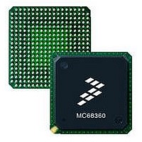
MC68EN360CAI25L Freescale Semiconductor, MC68EN360CAI25L Datasheet - Page 70

MC68EN360CAI25L
Manufacturer Part Number
MC68EN360CAI25L
Description
IC MPU QUICC 25MHZ 240-FQFP
Manufacturer
Freescale Semiconductor
Series
MC68000r
Datasheets
1.MC68EN302AG20BT.pdf
(8 pages)
2.MC68EN360VR25L.pdf
(14 pages)
3.MC68EN360VR25L.pdf
(2 pages)
4.MC68EN360CAI25L.pdf
(962 pages)
Specifications of MC68EN360CAI25L
Processor Type
M683xx 32-Bit
Speed
25MHz
Voltage
5V
Mounting Type
Surface Mount
Package / Case
240-FQFP
Core Size
32 Bit
Cpu Speed
25MHz
Embedded Interface Type
SCP, TDM
Digital Ic Case Style
FQFP
No. Of Pins
240
Supply Voltage Range
4.75V To 5.25V
Rohs Compliant
Yes
Family Name
M68xxx
Device Core
ColdFire
Device Core Size
32b
Frequency (max)
25MHz
Instruction Set Architecture
RISC
Supply Voltage 1 (typ)
5V
Operating Supply Voltage (max)
5.25V
Operating Supply Voltage (min)
4.75V
Operating Temp Range
-40C to 85C
Operating Temperature Classification
Industrial
Mounting
Surface Mount
Pin Count
240
Package Type
FQFP
Lead Free Status / RoHS Status
Lead free / RoHS Compliant
Features
-
Lead Free Status / Rohs Status
Compliant
Available stocks
Company
Part Number
Manufacturer
Quantity
Price
Company:
Part Number:
MC68EN360CAI25L
Manufacturer:
APLHA
Quantity:
12 000
Company:
Part Number:
MC68EN360CAI25L
Manufacturer:
Freescale Semiconductor
Quantity:
10 000
Part Number:
MC68EN360CAI25L
Manufacturer:
FREESCALE
Quantity:
20 000
- MC68EN302AG20BT PDF datasheet
- MC68EN360VR25L PDF datasheet #2
- MC68EN360VR25L PDF datasheet #3
- MC68EN360CAI25L PDF datasheet #4
- Current page: 70 of 962
- Download datasheet (4Mb)
QUICC Memory Map
3.3 INTERNAL REGISTERS MEMORY MAP
In addition to the internal dual-port RAM, there are a number of internal registers to support
the functions of the various CPU32+ core peripherals. The internal registers (see Table 3-3
and Table 3-4) are memory-mapped registers offset from the register base (REGBASE)
pointer. REGBASE (abbreviated REGB) = DPRBASE + 4K. All registers are located on the
internal IMB.
3.3.1 SIM Registers Memory Map
Table 3-3 lists the SIM registers memory map.
3-4
All registers that are underlined in the following tables are spe-
cial registers called event registers. In these registers, bits are
set by the QUICC and cleared by the user. To clear a bit, the
user must write a one to that bit. For example, to clear bit 2 in
SCCE1, the MOVE.B #$04,SCCE1 instruction may be used. Do
NOT use read-modify-write instructions (such as BSET, BCLR,
AND, OR, etc.) with these registers, or ALL bits in that register
will inadvertently be cleared. See the individual register descrip-
tions for more information.
All undefined and reserved bits within registers and parameter
RAM values written by the user should be written with zero to al-
low for future enhancements to the device.
Bold letters mark registers that are restricted to supervisor ac-
cess.
Table 3-2. CPM Sub-Module Base Addresses
Freescale Semiconductor, Inc.
3
4
4
4
For More Information On This Product,
MC68360 USER’S MANUAL
Go to: www.freescale.com
IDMA2 Base
SMC1 Base
SMC2 Base
SCC4 Base
NOTES
DPRBASE + $E80
DPRBASE + $F00
DPRBASE + $F70
DPRBASE + $F80
Related parts for MC68EN360CAI25L
Image
Part Number
Description
Manufacturer
Datasheet
Request
R
Part Number:
Description:
Manufacturer:
Freescale Semiconductor, Inc
Datasheet:
Part Number:
Description:
Manufacturer:
Freescale Semiconductor, Inc
Datasheet:
Part Number:
Description:
Manufacturer:
Freescale Semiconductor, Inc
Datasheet:
Part Number:
Description:
Manufacturer:
Freescale Semiconductor, Inc
Datasheet:
Part Number:
Description:
Manufacturer:
Freescale Semiconductor, Inc
Datasheet:
Part Number:
Description:
Manufacturer:
Freescale Semiconductor, Inc
Datasheet:
Part Number:
Description:
Manufacturer:
Freescale Semiconductor, Inc
Datasheet:
Part Number:
Description:
Manufacturer:
Freescale Semiconductor, Inc
Datasheet:
Part Number:
Description:
Manufacturer:
Freescale Semiconductor, Inc
Datasheet:
Part Number:
Description:
Manufacturer:
Freescale Semiconductor, Inc
Datasheet:
Part Number:
Description:
Manufacturer:
Freescale Semiconductor, Inc
Datasheet:
Part Number:
Description:
Manufacturer:
Freescale Semiconductor, Inc
Datasheet:
Part Number:
Description:
Manufacturer:
Freescale Semiconductor, Inc
Datasheet:
Part Number:
Description:
Manufacturer:
Freescale Semiconductor, Inc
Datasheet:
Part Number:
Description:
Manufacturer:
Freescale Semiconductor, Inc
Datasheet:


