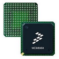
MC68EN360CAI25L Freescale Semiconductor, MC68EN360CAI25L Datasheet - Page 99

MC68EN360CAI25L
Manufacturer Part Number
MC68EN360CAI25L
Description
IC MPU QUICC 25MHZ 240-FQFP
Manufacturer
Freescale Semiconductor
Series
MC68000r
Datasheets
1.MC68EN302AG20BT.pdf
(8 pages)
2.MC68EN360VR25L.pdf
(14 pages)
3.MC68EN360VR25L.pdf
(2 pages)
4.MC68EN360CAI25L.pdf
(962 pages)
Specifications of MC68EN360CAI25L
Processor Type
M683xx 32-Bit
Speed
25MHz
Voltage
5V
Mounting Type
Surface Mount
Package / Case
240-FQFP
Core Size
32 Bit
Cpu Speed
25MHz
Embedded Interface Type
SCP, TDM
Digital Ic Case Style
FQFP
No. Of Pins
240
Supply Voltage Range
4.75V To 5.25V
Rohs Compliant
Yes
Family Name
M68xxx
Device Core
ColdFire
Device Core Size
32b
Frequency (max)
25MHz
Instruction Set Architecture
RISC
Supply Voltage 1 (typ)
5V
Operating Supply Voltage (max)
5.25V
Operating Supply Voltage (min)
4.75V
Operating Temp Range
-40C to 85C
Operating Temperature Classification
Industrial
Mounting
Surface Mount
Pin Count
240
Package Type
FQFP
Lead Free Status / RoHS Status
Lead free / RoHS Compliant
Features
-
Lead Free Status / Rohs Status
Compliant
Available stocks
Company
Part Number
Manufacturer
Quantity
Price
Company:
Part Number:
MC68EN360CAI25L
Manufacturer:
APLHA
Quantity:
12 000
Company:
Part Number:
MC68EN360CAI25L
Manufacturer:
Freescale Semiconductor
Quantity:
10 000
Part Number:
MC68EN360CAI25L
Manufacturer:
FREESCALE
Quantity:
20 000
- MC68EN302AG20BT PDF datasheet
- MC68EN360VR25L PDF datasheet #2
- MC68EN360VR25L PDF datasheet #3
- MC68EN360CAI25L PDF datasheet #4
- Current page: 99 of 962
- Download datasheet (4Mb)
4.3.1 Read Cycle
During a read cycle, the QUICC receives data from a memory or peripheral device. If the
instruction specifies a long-word operation, the QUICC attempts to read four bytes at once.
For a word operation, the QUICC attempts to read two bytes at once. For a byte operation,
the QUICC reads one byte. The section of the data bus from which each byte is read
depends on the operand size, address signals (A1, A0), and the port size. Refer to 4.2.1
Dynamic Bus Sizing and 4.2.2 Misaligned Operands for more information.
Figure 4-15 shows a long-word read cycle flowchart and Figure 4-16 illustrates a byte read
cycle flowchart. Figure 4-17 and Figure 4-18 show functional read cycles timing diagrams
specified in terms of clock periods.
2) NEGATE AS, DS, AND OE
1) SET R/W TO READ
2) DRIVE ADDRESS ON A31–A0
3) DRIVE FUNCTION CODE ON FC3–FC0
4) DRIVE SIZE (SIZ1–SIZ0) (ONE BYTE)
5) ASSERT AS, DS, AND OE
1) LATCH DATA
5) ASSERT AS, OE AND DS
1) SET R/W TO READ
2) DRIVE ADDRESS ON A31–A0
3) DRIVE FUNCTION CODE ON FC3–FC0
4) DRIVE SIZx PINS FOR FOUR BTYES
1) LATCH DATA
2) NEGATE AS, OE AND DS
TERMINATE OUTPUT TRANSFER
START NEXT CYCLE
ADDRESS DEVICE
START NEXT CYCLE
BUS MASTER
Figure 4-15. Long-Word Read Cycle Flowchart
ADDRESS DEVICE
ACQUIRE DATA
BUS MASTER
Freescale Semiconductor, Inc.
Figure 4-16. Byte Read Cycle Flowchart
For More Information On This Product,
MC68360 USER’S MANUAL
Go to: www.freescale.com
1) DECODE ADDRESS
2) PLACE DATA ON D31–D24, OR D23–16, OR
3) ASSERT DSACKx
1) REMOVE DATA FROM D31–D0
2) NEGATE DSACKx
1) DECODE ADDRESS
2) PLACE DATA ON D31–D0
3) DRIVE DSACKx SIGNALS
1) REMOVE DATA FROM D31–D0
2) NEGATE DSACKx
D15–D8, OR D7–D0.
TERMINATE CYCLE
EXTERNAL DEVICE
PRESENT DATA
TERMINATE CYCLE
PRESENT DATA
SLAVE
Bus Operation
Related parts for MC68EN360CAI25L
Image
Part Number
Description
Manufacturer
Datasheet
Request
R
Part Number:
Description:
Manufacturer:
Freescale Semiconductor, Inc
Datasheet:
Part Number:
Description:
Manufacturer:
Freescale Semiconductor, Inc
Datasheet:
Part Number:
Description:
Manufacturer:
Freescale Semiconductor, Inc
Datasheet:
Part Number:
Description:
Manufacturer:
Freescale Semiconductor, Inc
Datasheet:
Part Number:
Description:
Manufacturer:
Freescale Semiconductor, Inc
Datasheet:
Part Number:
Description:
Manufacturer:
Freescale Semiconductor, Inc
Datasheet:
Part Number:
Description:
Manufacturer:
Freescale Semiconductor, Inc
Datasheet:
Part Number:
Description:
Manufacturer:
Freescale Semiconductor, Inc
Datasheet:
Part Number:
Description:
Manufacturer:
Freescale Semiconductor, Inc
Datasheet:
Part Number:
Description:
Manufacturer:
Freescale Semiconductor, Inc
Datasheet:
Part Number:
Description:
Manufacturer:
Freescale Semiconductor, Inc
Datasheet:
Part Number:
Description:
Manufacturer:
Freescale Semiconductor, Inc
Datasheet:
Part Number:
Description:
Manufacturer:
Freescale Semiconductor, Inc
Datasheet:
Part Number:
Description:
Manufacturer:
Freescale Semiconductor, Inc
Datasheet:
Part Number:
Description:
Manufacturer:
Freescale Semiconductor, Inc
Datasheet:


