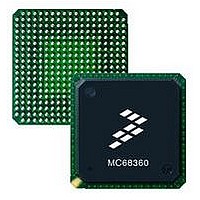
MC68EN360CAI25L Freescale Semiconductor, MC68EN360CAI25L Datasheet - Page 302

MC68EN360CAI25L
Manufacturer Part Number
MC68EN360CAI25L
Description
IC MPU QUICC 25MHZ 240-FQFP
Manufacturer
Freescale Semiconductor
Series
MC68000r
Datasheets
1.MC68EN302AG20BT.pdf
(8 pages)
2.MC68EN360VR25L.pdf
(14 pages)
3.MC68EN360VR25L.pdf
(2 pages)
4.MC68EN360CAI25L.pdf
(962 pages)
Specifications of MC68EN360CAI25L
Processor Type
M683xx 32-Bit
Speed
25MHz
Voltage
5V
Mounting Type
Surface Mount
Package / Case
240-FQFP
Core Size
32 Bit
Cpu Speed
25MHz
Embedded Interface Type
SCP, TDM
Digital Ic Case Style
FQFP
No. Of Pins
240
Supply Voltage Range
4.75V To 5.25V
Rohs Compliant
Yes
Family Name
M68xxx
Device Core
ColdFire
Device Core Size
32b
Frequency (max)
25MHz
Instruction Set Architecture
RISC
Supply Voltage 1 (typ)
5V
Operating Supply Voltage (max)
5.25V
Operating Supply Voltage (min)
4.75V
Operating Temp Range
-40C to 85C
Operating Temperature Classification
Industrial
Mounting
Surface Mount
Pin Count
240
Package Type
FQFP
Lead Free Status / RoHS Status
Lead free / RoHS Compliant
Features
-
Lead Free Status / Rohs Status
Compliant
Available stocks
Company
Part Number
Manufacturer
Quantity
Price
Company:
Part Number:
MC68EN360CAI25L
Manufacturer:
APLHA
Quantity:
12 000
Company:
Part Number:
MC68EN360CAI25L
Manufacturer:
Freescale Semiconductor
Quantity:
10 000
Part Number:
MC68EN360CAI25L
Manufacturer:
FREESCALE
Quantity:
20 000
- MC68EN302AG20BT PDF datasheet
- MC68EN360VR25L PDF datasheet #2
- MC68EN360VR25L PDF datasheet #3
- MC68EN360CAI25L PDF datasheet #4
- Current page: 302 of 962
- Download datasheet (4Mb)
Freescale Semiconductor, Inc.
System Integration Module (SIM60)
When more wait states are programmed into the TCYC bits of the OR, the external AS (or
TS line) is synchronized internally.
The BADDR3–BADDR2 signals equal the A3–A2 signals when a burst is not in progress.
This configuration allows a non-bursting master to access the same memory as a bursting
external master by using the BADDR3–BADDR2 signals.
6.11.8 Global (Boot) Chip-Select Operation
Global (boot) chip-select operation allows address decoding for a boot ROM before system
initialization occurs. CS0 is the global chip-select output. Its operation differs from the other
external chip-select outputs following a system reset. When the CPU32+ begins accessing
memory after a system reset, CS0 is asserted for every address, unless the MBAR is
accessed or an internal peripheral on the IMB is accessed.
The global chip select provides a programmable port size at system reset using the CONFIG
pins. This capability allows a boot ROM to be located anywhere in the address space (with
up to 14 wait states), while still providing the stack pointer and program counter values at
$00000000 and $00000004, respectively. The global chip select does not provide write pro-
tection and responds to all function codes. CS0 operates in this manner until the first write
to the CS0 option register (OR0). CS0 can be programmed to continue decoding a range of
addresses after this write, provided the desired address range is first loaded into base reg-
ister 0. After the first write to the OR0, the global chip select can only be restarted with a
system reset.
6.11.9 SRAM Bus Error
The BERR signal may be asserted by the SRAM controller in the case of a parity error or by
the bus monitor of the SIM60 as a result of a write-protect violation. In addition, if the BERR
signal is asserted externally, it should not be asserted until at least S2 of the bus cycle.
6.12 DRAM CONTROLLER OVERVIEW (DRAM BANKS)
The DRAM controller supports a glueless interface to 16-bit (18 bit with parity) or 32-bit (36
bit with parity) DRAM or DRAM SIMMs from an internal QUICC master (CPU32+, IDMAs,
SDMAs). Many different DRAM bank sizes are supported: 128K, 256K, 512K, 1M, 2M, 4M,
8M, and 16M; thus, DRAMs such as 128K x 8, and 16M x 4 are supported. The DRAM con-
troller performs the address multiplexing for internal masters using the low-order address
lines.
Table 6-8 lists the physical address lines of the DRAM (row and column). In the case of a
16-bit DRAM port size with a 512K DRAM device (e.g., two 512K x 8 devices for a total of
16 bits wide), the row address to the DRAM bank will be A19–A10, and the column address
to the DRAM bank will be A9–A1. However, these signals will be internally multiplexed on
the A10–A1 pins; thus, the user should connect A10–A1 to the address pins on each 512K
DRAM device.
6-58
MC68360 USER’S MANUAL
For More Information On This Product,
Go to: www.freescale.com
Related parts for MC68EN360CAI25L
Image
Part Number
Description
Manufacturer
Datasheet
Request
R
Part Number:
Description:
Manufacturer:
Freescale Semiconductor, Inc
Datasheet:
Part Number:
Description:
Manufacturer:
Freescale Semiconductor, Inc
Datasheet:
Part Number:
Description:
Manufacturer:
Freescale Semiconductor, Inc
Datasheet:
Part Number:
Description:
Manufacturer:
Freescale Semiconductor, Inc
Datasheet:
Part Number:
Description:
Manufacturer:
Freescale Semiconductor, Inc
Datasheet:
Part Number:
Description:
Manufacturer:
Freescale Semiconductor, Inc
Datasheet:
Part Number:
Description:
Manufacturer:
Freescale Semiconductor, Inc
Datasheet:
Part Number:
Description:
Manufacturer:
Freescale Semiconductor, Inc
Datasheet:
Part Number:
Description:
Manufacturer:
Freescale Semiconductor, Inc
Datasheet:
Part Number:
Description:
Manufacturer:
Freescale Semiconductor, Inc
Datasheet:
Part Number:
Description:
Manufacturer:
Freescale Semiconductor, Inc
Datasheet:
Part Number:
Description:
Manufacturer:
Freescale Semiconductor, Inc
Datasheet:
Part Number:
Description:
Manufacturer:
Freescale Semiconductor, Inc
Datasheet:
Part Number:
Description:
Manufacturer:
Freescale Semiconductor, Inc
Datasheet:
Part Number:
Description:
Manufacturer:
Freescale Semiconductor, Inc
Datasheet:


