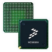
MC68EN360CAI25L Freescale Semiconductor, MC68EN360CAI25L Datasheet - Page 237

MC68EN360CAI25L
Manufacturer Part Number
MC68EN360CAI25L
Description
IC MPU QUICC 25MHZ 240-FQFP
Manufacturer
Freescale Semiconductor
Series
MC68000r
Datasheets
1.MC68EN302AG20BT.pdf
(8 pages)
2.MC68EN360VR25L.pdf
(14 pages)
3.MC68EN360VR25L.pdf
(2 pages)
4.MC68EN360CAI25L.pdf
(962 pages)
Specifications of MC68EN360CAI25L
Processor Type
M683xx 32-Bit
Speed
25MHz
Voltage
5V
Mounting Type
Surface Mount
Package / Case
240-FQFP
Core Size
32 Bit
Cpu Speed
25MHz
Embedded Interface Type
SCP, TDM
Digital Ic Case Style
FQFP
No. Of Pins
240
Supply Voltage Range
4.75V To 5.25V
Rohs Compliant
Yes
Family Name
M68xxx
Device Core
ColdFire
Device Core Size
32b
Frequency (max)
25MHz
Instruction Set Architecture
RISC
Supply Voltage 1 (typ)
5V
Operating Supply Voltage (max)
5.25V
Operating Supply Voltage (min)
4.75V
Operating Temp Range
-40C to 85C
Operating Temperature Classification
Industrial
Mounting
Surface Mount
Pin Count
240
Package Type
FQFP
Lead Free Status / RoHS Status
Lead free / RoHS Compliant
Features
-
Lead Free Status / Rohs Status
Compliant
Available stocks
Company
Part Number
Manufacturer
Quantity
Price
Company:
Part Number:
MC68EN360CAI25L
Manufacturer:
APLHA
Quantity:
12 000
Company:
Part Number:
MC68EN360CAI25L
Manufacturer:
Freescale Semiconductor
Quantity:
10 000
Part Number:
MC68EN360CAI25L
Manufacturer:
FREESCALE
Quantity:
20 000
- MC68EN302AG20BT PDF datasheet
- MC68EN360VR25L PDF datasheet #2
- MC68EN360VR25L PDF datasheet #3
- MC68EN360CAI25L PDF datasheet #4
- Current page: 237 of 962
- Download datasheet (4Mb)
5.7.2.6 IMMEDIATE ARITHMETIC/LOGIC INSTRUCTIONS. The immediate arithmetic/
logic instruction table indicates the number of clock periods needed for the processor to
fetch the source immediate data value and to perform the specified arithmetic/logic instruc-
tion using the specified addressing mode. Footnotes indicate when to account for the appro-
priate fetch effective or fetch immediate EA times. The total number of clock cycles is
outside the parentheses. The numbers inside parentheses (r/p/w) are included in the total
clock cycle number. All timing data assumes two-clock reads and writes.
5.7.2.7 BINARY-CODED DECIMAL AND EXTENDED INSTRUCTIONS. The BCD and
extended instruction table indicates the number of clock periods needed for the processor
to perform the specified operation using the specified addressing mode. No additional tables
are needed to calculate total effective execution time for these instructions. The total number
of clock cycles is outside the parentheses. The numbers inside parentheses (r/p/w) are
included in the total clock cycle number. All timing data assumes two-clock reads and writes.
MOVEQ#, Dn
ADDQ
ADDQ
SUBQ
SUBQ
ADDI
ADDI
ANDI
ANDI
EORI
EORI
ORI
ORI
SUBI
SUBI
CMPI
CMPI
X = There is one bus cycle for byte and word operands and two bus cycles for long-word op-
X = There is one bus cycle for byte and word operands and two bus cycles for long operands.
su = The execution time is identical for signed or unsigned operands.
*
= An # fetch EA time must be added for this instruction: FEA
= Maximum time (certain data or mode combinations may execute faster).
= These instructions have an additional save operation that other instructions do not have.
erands. For long-word bus cycles, add two clocks to the tail and to the number of cycles.
Timing is calculated with the CPU32+ in 16-bit mode.
For long bus cycles, add two clocks to the tail and to the number of cycles.
Timing is calculated with the CPU32+ in 16-bit mode.
To calculate total instruction time, calculate save, ea , and operation execution times,
then combine in the order listed, using equations in 5.7.1.6 Instruction Execution Time
Calculation. A save operation is not run for long-word divide and multiply instructions
when FEA
#, Rn
#, FEA
#, Rn
#, FEA
#, Rn
#, FEA
#, Rn
#, FEA
#, Rn
#, FEA
#, Rn
#, FEA
#, Rn
#, FEA
#, Rn
#, FEA
Instruction
Freescale Semiconductor, Inc.
For More Information On This Product,
Dn.
MC68360 USER’S MANUAL
Go to: www.freescale.com
Head
0
0
0
0
0
0
0
0
0
0
0
0
0
0
0
0
0
Tail
0
0
3
0
3
0
3
0
3
0
3
0
3
0
3
0
3
FEA
OPER
2(0/1/0)
2(0/1/0)
2(0/1/0)
2(0/1/0)
2(0/1/0)
2(0/1/0)
5(0/1/x)
5(0/1/x)
5(0/1/x)
5(0/1/x)
5(0/1/x)
5(0/1/x)
2(0/1/0)
2(0/1/0)
5(0/1/x)
2(0/1/0)
5(0/1/x)
Cycles
CPU32+
Related parts for MC68EN360CAI25L
Image
Part Number
Description
Manufacturer
Datasheet
Request
R
Part Number:
Description:
Manufacturer:
Freescale Semiconductor, Inc
Datasheet:
Part Number:
Description:
Manufacturer:
Freescale Semiconductor, Inc
Datasheet:
Part Number:
Description:
Manufacturer:
Freescale Semiconductor, Inc
Datasheet:
Part Number:
Description:
Manufacturer:
Freescale Semiconductor, Inc
Datasheet:
Part Number:
Description:
Manufacturer:
Freescale Semiconductor, Inc
Datasheet:
Part Number:
Description:
Manufacturer:
Freescale Semiconductor, Inc
Datasheet:
Part Number:
Description:
Manufacturer:
Freescale Semiconductor, Inc
Datasheet:
Part Number:
Description:
Manufacturer:
Freescale Semiconductor, Inc
Datasheet:
Part Number:
Description:
Manufacturer:
Freescale Semiconductor, Inc
Datasheet:
Part Number:
Description:
Manufacturer:
Freescale Semiconductor, Inc
Datasheet:
Part Number:
Description:
Manufacturer:
Freescale Semiconductor, Inc
Datasheet:
Part Number:
Description:
Manufacturer:
Freescale Semiconductor, Inc
Datasheet:
Part Number:
Description:
Manufacturer:
Freescale Semiconductor, Inc
Datasheet:
Part Number:
Description:
Manufacturer:
Freescale Semiconductor, Inc
Datasheet:
Part Number:
Description:
Manufacturer:
Freescale Semiconductor, Inc
Datasheet:


