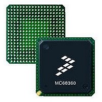
MC68EN360CAI25L Freescale Semiconductor, MC68EN360CAI25L Datasheet - Page 404

MC68EN360CAI25L
Manufacturer Part Number
MC68EN360CAI25L
Description
IC MPU QUICC 25MHZ 240-FQFP
Manufacturer
Freescale Semiconductor
Series
MC68000r
Datasheets
1.MC68EN302AG20BT.pdf
(8 pages)
2.MC68EN360VR25L.pdf
(14 pages)
3.MC68EN360VR25L.pdf
(2 pages)
4.MC68EN360CAI25L.pdf
(962 pages)
Specifications of MC68EN360CAI25L
Processor Type
M683xx 32-Bit
Speed
25MHz
Voltage
5V
Mounting Type
Surface Mount
Package / Case
240-FQFP
Core Size
32 Bit
Cpu Speed
25MHz
Embedded Interface Type
SCP, TDM
Digital Ic Case Style
FQFP
No. Of Pins
240
Supply Voltage Range
4.75V To 5.25V
Rohs Compliant
Yes
Family Name
M68xxx
Device Core
ColdFire
Device Core Size
32b
Frequency (max)
25MHz
Instruction Set Architecture
RISC
Supply Voltage 1 (typ)
5V
Operating Supply Voltage (max)
5.25V
Operating Supply Voltage (min)
4.75V
Operating Temp Range
-40C to 85C
Operating Temperature Classification
Industrial
Mounting
Surface Mount
Pin Count
240
Package Type
FQFP
Lead Free Status / RoHS Status
Lead free / RoHS Compliant
Features
-
Lead Free Status / Rohs Status
Compliant
Available stocks
Company
Part Number
Manufacturer
Quantity
Price
Company:
Part Number:
MC68EN360CAI25L
Manufacturer:
APLHA
Quantity:
12 000
Company:
Part Number:
MC68EN360CAI25L
Manufacturer:
Freescale Semiconductor
Quantity:
10 000
Part Number:
MC68EN360CAI25L
Manufacturer:
FREESCALE
Quantity:
20 000
- MC68EN302AG20BT PDF datasheet
- MC68EN360VR25L PDF datasheet #2
- MC68EN360VR25L PDF datasheet #3
- MC68EN360CAI25L PDF datasheet #4
- Current page: 404 of 962
- Download datasheet (4Mb)
Serial Interface with Time Slot Assigner
RFSDx—Receive Frame Sync Delay for TDM A or B
DSCx—Double-Speed Clock for TDM A or B
CRTx—Common Receive and Transmit Pins for TDM A or B
STZx—Set L1TXDx to Zero for TDM A or B
CEx—Clock Edge for TDM A or B
7-80
These two bits determine the number of clock delays between the receive sync and the
first bit of the receive frame. Even if the CRTx bit is set, these bits do not control the delay
for the transmit frame.
Refer to Figure 7-29 and Figure 7-30 for an example of the use of these bits.
Some TDMs such as GCI define the input clock to be 2 faster than the data rate. This bit
controls this option.
This bit is useful when the transmit and receive sections of a given TDM use the same
clock and sync signals. In this mode, L1TCLKx and L1TSYNCx pins can be used as gen-
eral-purpose I/O pins.
00 = No bit delay (The first bit of the frame is transmitted/received on the same clock
01 = 1-bit delay (Use for IDL.)
10 = 2-bit delay
11 = 3-bit delay
0 = The channel clock (L1RCLKx and/or L1TCLKx) is equal to the data clock. (Use for
1 = The channel clock rate is twice the data rate. (Use for GCI.)
0 = Separate pins. The receive section of this TDM uses L1RCLKx and L1RSYNCx
1 = Common pins. The receive and transmit sections of this TDM use L1RCLKx as
0 = Normal operation.
1 = L1TXDx is set to zero until serial clocks are available, which is useful for GCI acti-
When DSCx =0
0 = The data is transmitted on the rising edge of the clock and received on the falling
1 = The data is transmitted on the falling edge of the clock and received on the rising
When DSCx = 1
0 = The data is transmitted on the rising edge of the clock and received on the rising
1 = The data is transmitted on the falling edge of the clock and received on the falling
IDL and most TDM formats.)
pins for framing, and the transmit section uses L1TCLKx and L1TSYNCx for fram-
ing.
clock pin of channel x and L1RSYNCx as the receive and transmit sync pin. (Use
for IDL and GCI.)
vation. Refer to 7.8.7.1 SI GCI Activation/Deactivation Procedure.
edge. (Use for IDL and GCI.)
edge.
edge. (Use for IDL and GCI.)
edge.
as the sync; use for GCI.)
Freescale Semiconductor, Inc.
For More Information On This Product,
MC68360 USER’S MANUAL
Go to: www.freescale.com
Related parts for MC68EN360CAI25L
Image
Part Number
Description
Manufacturer
Datasheet
Request
R
Part Number:
Description:
Manufacturer:
Freescale Semiconductor, Inc
Datasheet:
Part Number:
Description:
Manufacturer:
Freescale Semiconductor, Inc
Datasheet:
Part Number:
Description:
Manufacturer:
Freescale Semiconductor, Inc
Datasheet:
Part Number:
Description:
Manufacturer:
Freescale Semiconductor, Inc
Datasheet:
Part Number:
Description:
Manufacturer:
Freescale Semiconductor, Inc
Datasheet:
Part Number:
Description:
Manufacturer:
Freescale Semiconductor, Inc
Datasheet:
Part Number:
Description:
Manufacturer:
Freescale Semiconductor, Inc
Datasheet:
Part Number:
Description:
Manufacturer:
Freescale Semiconductor, Inc
Datasheet:
Part Number:
Description:
Manufacturer:
Freescale Semiconductor, Inc
Datasheet:
Part Number:
Description:
Manufacturer:
Freescale Semiconductor, Inc
Datasheet:
Part Number:
Description:
Manufacturer:
Freescale Semiconductor, Inc
Datasheet:
Part Number:
Description:
Manufacturer:
Freescale Semiconductor, Inc
Datasheet:
Part Number:
Description:
Manufacturer:
Freescale Semiconductor, Inc
Datasheet:
Part Number:
Description:
Manufacturer:
Freescale Semiconductor, Inc
Datasheet:
Part Number:
Description:
Manufacturer:
Freescale Semiconductor, Inc
Datasheet:


