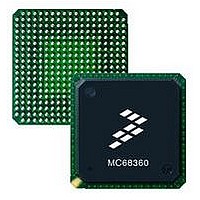
MC68EN360CAI25L Freescale Semiconductor, MC68EN360CAI25L Datasheet - Page 268

MC68EN360CAI25L
Manufacturer Part Number
MC68EN360CAI25L
Description
IC MPU QUICC 25MHZ 240-FQFP
Manufacturer
Freescale Semiconductor
Series
MC68000r
Datasheets
1.MC68EN302AG20BT.pdf
(8 pages)
2.MC68EN360VR25L.pdf
(14 pages)
3.MC68EN360VR25L.pdf
(2 pages)
4.MC68EN360CAI25L.pdf
(962 pages)
Specifications of MC68EN360CAI25L
Processor Type
M683xx 32-Bit
Speed
25MHz
Voltage
5V
Mounting Type
Surface Mount
Package / Case
240-FQFP
Core Size
32 Bit
Cpu Speed
25MHz
Embedded Interface Type
SCP, TDM
Digital Ic Case Style
FQFP
No. Of Pins
240
Supply Voltage Range
4.75V To 5.25V
Rohs Compliant
Yes
Family Name
M68xxx
Device Core
ColdFire
Device Core Size
32b
Frequency (max)
25MHz
Instruction Set Architecture
RISC
Supply Voltage 1 (typ)
5V
Operating Supply Voltage (max)
5.25V
Operating Supply Voltage (min)
4.75V
Operating Temp Range
-40C to 85C
Operating Temperature Classification
Industrial
Mounting
Surface Mount
Pin Count
240
Package Type
FQFP
Lead Free Status / RoHS Status
Lead free / RoHS Compliant
Features
-
Lead Free Status / Rohs Status
Compliant
Available stocks
Company
Part Number
Manufacturer
Quantity
Price
Company:
Part Number:
MC68EN360CAI25L
Manufacturer:
APLHA
Quantity:
12 000
Company:
Part Number:
MC68EN360CAI25L
Manufacturer:
Freescale Semiconductor
Quantity:
10 000
Part Number:
MC68EN360CAI25L
Manufacturer:
FREESCALE
Quantity:
20 000
- MC68EN302AG20BT PDF datasheet
- MC68EN360VR25L PDF datasheet #2
- MC68EN360VR25L PDF datasheet #3
- MC68EN360CAI25L PDF datasheet #4
- Current page: 268 of 962
- Download datasheet (4Mb)
System Integration Module (SIM60)
6.8.1 MBAR in a Multiple QUICC System
The module base address register (MBAR) is used to configure the location of the QUICC's
block of on-chip RAM and registers. In a multiple QUICC system, a technique must be pro-
vided to allow multiple MBARs on multiple QUICCs to be programmed with unique values.
The QUICC has several provisions to support this.
First, any QUICC that is configured into slave mode with its global chip select disabled
(CONFIG pins = 110) automatically has its MBAR location changed from $0003FF00 to
$0003FF04. Second, the MBAR, newly located at address $0003FF04, can only be enabled
for access after a keyed write operation is performed (see Figure 6-9). The keyed write
allows the user to program the MBARs of multiple QUICC slaves without adding any exter-
nal glue logic.
6-24
4 KB
4 KB
Figure 6-9. MBAR Access to a Multiple QUICC Slave System
When used in slave mode, the QUICC must be configured with
a 32-bit data bus.
Even without the use of the slave mode, another processor can
be granted access to the QUICC's on-chip peripherals by re-
questing the bus with the BR pin.
If the QUICC is configured into slave mode with its global chip
select enabled, the MBAR location does not change, and the
keyed write is not required. Thus, a single QUICC configured as
a slave to an MC68EC040 or MC68EC030 does not require a
keyed write for its MBAR.
If there are N QUICCs sharing a bus, N–1 QUICCs would nor-
mally have their CONFIG pins configured as 110.
DUAL-PORT
REGISTERS
INTERNAL
RAM
Freescale Semiconductor, Inc.
For More Information On This Product,
MC68360 USER’S MANUAL
Go to: www.freescale.com
NOTES
NOTES
MBARE
MBAR
MBAR SELECT BIT (BIT 31)
$0003FF04; FC = 111
$0003FF08; FC = 111
MBARE PIN
Related parts for MC68EN360CAI25L
Image
Part Number
Description
Manufacturer
Datasheet
Request
R
Part Number:
Description:
Manufacturer:
Freescale Semiconductor, Inc
Datasheet:
Part Number:
Description:
Manufacturer:
Freescale Semiconductor, Inc
Datasheet:
Part Number:
Description:
Manufacturer:
Freescale Semiconductor, Inc
Datasheet:
Part Number:
Description:
Manufacturer:
Freescale Semiconductor, Inc
Datasheet:
Part Number:
Description:
Manufacturer:
Freescale Semiconductor, Inc
Datasheet:
Part Number:
Description:
Manufacturer:
Freescale Semiconductor, Inc
Datasheet:
Part Number:
Description:
Manufacturer:
Freescale Semiconductor, Inc
Datasheet:
Part Number:
Description:
Manufacturer:
Freescale Semiconductor, Inc
Datasheet:
Part Number:
Description:
Manufacturer:
Freescale Semiconductor, Inc
Datasheet:
Part Number:
Description:
Manufacturer:
Freescale Semiconductor, Inc
Datasheet:
Part Number:
Description:
Manufacturer:
Freescale Semiconductor, Inc
Datasheet:
Part Number:
Description:
Manufacturer:
Freescale Semiconductor, Inc
Datasheet:
Part Number:
Description:
Manufacturer:
Freescale Semiconductor, Inc
Datasheet:
Part Number:
Description:
Manufacturer:
Freescale Semiconductor, Inc
Datasheet:
Part Number:
Description:
Manufacturer:
Freescale Semiconductor, Inc
Datasheet:


