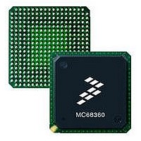
MC68EN360CAI25L Freescale Semiconductor, MC68EN360CAI25L Datasheet - Page 295

MC68EN360CAI25L
Manufacturer Part Number
MC68EN360CAI25L
Description
IC MPU QUICC 25MHZ 240-FQFP
Manufacturer
Freescale Semiconductor
Series
MC68000r
Datasheets
1.MC68EN302AG20BT.pdf
(8 pages)
2.MC68EN360VR25L.pdf
(14 pages)
3.MC68EN360VR25L.pdf
(2 pages)
4.MC68EN360CAI25L.pdf
(962 pages)
Specifications of MC68EN360CAI25L
Processor Type
M683xx 32-Bit
Speed
25MHz
Voltage
5V
Mounting Type
Surface Mount
Package / Case
240-FQFP
Core Size
32 Bit
Cpu Speed
25MHz
Embedded Interface Type
SCP, TDM
Digital Ic Case Style
FQFP
No. Of Pins
240
Supply Voltage Range
4.75V To 5.25V
Rohs Compliant
Yes
Family Name
M68xxx
Device Core
ColdFire
Device Core Size
32b
Frequency (max)
25MHz
Instruction Set Architecture
RISC
Supply Voltage 1 (typ)
5V
Operating Supply Voltage (max)
5.25V
Operating Supply Voltage (min)
4.75V
Operating Temp Range
-40C to 85C
Operating Temperature Classification
Industrial
Mounting
Surface Mount
Pin Count
240
Package Type
FQFP
Lead Free Status / RoHS Status
Lead free / RoHS Compliant
Features
-
Lead Free Status / Rohs Status
Compliant
Available stocks
Company
Part Number
Manufacturer
Quantity
Price
Company:
Part Number:
MC68EN360CAI25L
Manufacturer:
APLHA
Quantity:
12 000
Company:
Part Number:
MC68EN360CAI25L
Manufacturer:
Freescale Semiconductor
Quantity:
10 000
Part Number:
MC68EN360CAI25L
Manufacturer:
FREESCALE
Quantity:
20 000
- MC68EN302AG20BT PDF datasheet
- MC68EN360VR25L PDF datasheet #2
- MC68EN360VR25L PDF datasheet #3
- MC68EN360CAI25L PDF datasheet #4
- Current page: 295 of 962
- Download datasheet (4Mb)
6.10.2 Memory Controller Overview
The block diagram of the QUICC memory controller is shown in Figure 6-10. The general-
purpose chip selects provide a glueless interface to EPROM, SRAM, flash EPROM
(FEPROM), and other peripherals. The general-purpose chip selects are available on lines
CS0–CS7. CS0 also functions as the global (boot) chip select for accessing the boot
EPROM. The chip selects allow 0 to 15 wait states.
The flexible memory controller allows a glueless DRAM interface to single in-line memory
modules (SIMMs) as well as a grid array of DRAMs on a board. The DRAM controller con-
trols the address multiplexing, access mode, refresh operation, and the timing generation
• General-Purpose Chip Selects (SRAM Banks)
• DRAM Controller (DRAM Banks)
• DRAM Controller Also Contains a Refresh Unit with:
• DRAM Controller Also Supports External Masters
—May Be Used with SRAM, EPROM, FEPROM, and Peripherals
—Global (Boot) Chip Select Available at System Reset
—Two-Clock Accesses to External SRAM
—Programmable Port Size of 8, 16, and 32 Bits for Each Chip Select
—Supports up to Eight Banks of DRAM of Size 128K
—Supports a DRAM Port Size of 16 or 32 Bits
—Internal Address Multiplexing for 16- and 32-Bit DRAM Systems Available for all On-
—Glueless Interface to One Bank of DRAM SIMMs (Only External Buffers Are Re-
—Four CAS Lines
—Two of the Eight RAS Lines May Be Output on Two Pins Each for Double-Drive Ca-
—Page Mode with Page Switch Detection Logic
—Page Mode Supports 128K, 256K, 512K, 1M, 2M, 4M, 8M, and 16M Page Banks
—Supports Page Mode Normal, Page Hit, and Page Miss
—Burst Support for the MC68040 Accesses to DRAM
—CAS Before RAS Refresh Support
—A Programmable Refresh Timer
—Refresh Active During External Reset
—Disable Refresh Mode
—Stacking of up to Seven Refresh Cycles
—Supports MC68EC040 with 3,2,2,2 Line Fill (60-ns DRAMs)
—Supports DRAM for External QUICC or MC68030-Type Accesses (Page Support
—Supports DRAM Control for System Bus Containing External MC68EC040 and Mul-
—Synchronous and Asynchronous External Masters Possible
—Special Options for External Master to Improve DRAM Performance
1M
Chip Bus Masters
quired for Additional SIMM Banks)
pability
Available in this Mode)
tiple QUICCs
X, 2M
X, 4M
Freescale Semiconductor, Inc.
For More Information On This Product,
X, 8M
MC68360 USER’S MANUAL
Go to: www.freescale.com
X or 16M
X
System Integration Module (SIM60)
X, 256K
X, 512K
X,
Related parts for MC68EN360CAI25L
Image
Part Number
Description
Manufacturer
Datasheet
Request
R
Part Number:
Description:
Manufacturer:
Freescale Semiconductor, Inc
Datasheet:
Part Number:
Description:
Manufacturer:
Freescale Semiconductor, Inc
Datasheet:
Part Number:
Description:
Manufacturer:
Freescale Semiconductor, Inc
Datasheet:
Part Number:
Description:
Manufacturer:
Freescale Semiconductor, Inc
Datasheet:
Part Number:
Description:
Manufacturer:
Freescale Semiconductor, Inc
Datasheet:
Part Number:
Description:
Manufacturer:
Freescale Semiconductor, Inc
Datasheet:
Part Number:
Description:
Manufacturer:
Freescale Semiconductor, Inc
Datasheet:
Part Number:
Description:
Manufacturer:
Freescale Semiconductor, Inc
Datasheet:
Part Number:
Description:
Manufacturer:
Freescale Semiconductor, Inc
Datasheet:
Part Number:
Description:
Manufacturer:
Freescale Semiconductor, Inc
Datasheet:
Part Number:
Description:
Manufacturer:
Freescale Semiconductor, Inc
Datasheet:
Part Number:
Description:
Manufacturer:
Freescale Semiconductor, Inc
Datasheet:
Part Number:
Description:
Manufacturer:
Freescale Semiconductor, Inc
Datasheet:
Part Number:
Description:
Manufacturer:
Freescale Semiconductor, Inc
Datasheet:
Part Number:
Description:
Manufacturer:
Freescale Semiconductor, Inc
Datasheet:


