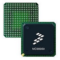
MC68EN360CAI25L Freescale Semiconductor, MC68EN360CAI25L Datasheet - Page 392

MC68EN360CAI25L
Manufacturer Part Number
MC68EN360CAI25L
Description
IC MPU QUICC 25MHZ 240-FQFP
Manufacturer
Freescale Semiconductor
Series
MC68000r
Datasheets
1.MC68EN302AG20BT.pdf
(8 pages)
2.MC68EN360VR25L.pdf
(14 pages)
3.MC68EN360VR25L.pdf
(2 pages)
4.MC68EN360CAI25L.pdf
(962 pages)
Specifications of MC68EN360CAI25L
Processor Type
M683xx 32-Bit
Speed
25MHz
Voltage
5V
Mounting Type
Surface Mount
Package / Case
240-FQFP
Core Size
32 Bit
Cpu Speed
25MHz
Embedded Interface Type
SCP, TDM
Digital Ic Case Style
FQFP
No. Of Pins
240
Supply Voltage Range
4.75V To 5.25V
Rohs Compliant
Yes
Family Name
M68xxx
Device Core
ColdFire
Device Core Size
32b
Frequency (max)
25MHz
Instruction Set Architecture
RISC
Supply Voltage 1 (typ)
5V
Operating Supply Voltage (max)
5.25V
Operating Supply Voltage (min)
4.75V
Operating Temp Range
-40C to 85C
Operating Temperature Classification
Industrial
Mounting
Surface Mount
Pin Count
240
Package Type
FQFP
Lead Free Status / RoHS Status
Lead free / RoHS Compliant
Features
-
Lead Free Status / Rohs Status
Compliant
Available stocks
Company
Part Number
Manufacturer
Quantity
Price
Company:
Part Number:
MC68EN360CAI25L
Manufacturer:
APLHA
Quantity:
12 000
Company:
Part Number:
MC68EN360CAI25L
Manufacturer:
Freescale Semiconductor
Quantity:
10 000
Part Number:
MC68EN360CAI25L
Manufacturer:
FREESCALE
Quantity:
20 000
- MC68EN302AG20BT PDF datasheet
- MC68EN360VR25L PDF datasheet #2
- MC68EN360VR25L PDF datasheet #3
- MC68EN360CAI25L PDF datasheet #4
- Current page: 392 of 962
- Download datasheet (4Mb)
Serial Interface with Time Slot Assigner
Once the connections are made, the exact routing decisions are made in the SI RAM, as
described in the following paragraphs.
7.8.4 SI RAM
The SI has two 64
SCCs and SMCs. The RAMs are uninitialized after power-on. For proper operation, the host
should program the RAMs before enabling the multiplexed channels, or undesired results
may occur.
The RAM consists of 16-bit entries that are used to define the routing control. Each entry
can control from 1 to 16 bits or from 1 to 16 bytes at a time as determined in the entry. In
addition to the routing, up to four strobe pins may be asserted according to the programming
of the RAM. The strobes are active high.
The two SI RAMs can be configured in four different ways to support various TDM channels.
The four possible cases are discussed in the following paragraphs.
7-68
NOTES:
SCC 1
SCC 2
SCC 3
SCC 4
SMC 1
SMC 2
1. The ENx bits are located in SIGMR.
2. The SCx bits are located in SICR.
3. The SMCx bits are located in SIMODE.
4. The clocking paths are not shown for the nonmultiplexed I/F (see Figure 7-35 for more details).
Figure 7-22. Enabling Connections Through the SI
16 static RAMs used to control the routing of the TDM channels to the
SI RAM
Freescale Semiconductor, Inc.
For More Information On This Product,
MC68360 USER’S MANUAL
Go to: www.freescale.com
CONTROL LOGIC
TIME SLOT
ASSIGNER
EN
EN
SC1=0
SC2=0
SMC2=0
SC3=0
SC4=0
SMC1=0
ENa = 1 TO ENABLE
ENb = 1 TO ENABLE
SCC3 PINS
SCC4 PINS
SCC1 PINS
SCC2 PINS
SMC1 PINS
SMC2 PINS
TDMa PINS
TDMb PINS
MULTIPLEXED
NONMULTIPLEXED
I/F
I/F
Related parts for MC68EN360CAI25L
Image
Part Number
Description
Manufacturer
Datasheet
Request
R
Part Number:
Description:
Manufacturer:
Freescale Semiconductor, Inc
Datasheet:
Part Number:
Description:
Manufacturer:
Freescale Semiconductor, Inc
Datasheet:
Part Number:
Description:
Manufacturer:
Freescale Semiconductor, Inc
Datasheet:
Part Number:
Description:
Manufacturer:
Freescale Semiconductor, Inc
Datasheet:
Part Number:
Description:
Manufacturer:
Freescale Semiconductor, Inc
Datasheet:
Part Number:
Description:
Manufacturer:
Freescale Semiconductor, Inc
Datasheet:
Part Number:
Description:
Manufacturer:
Freescale Semiconductor, Inc
Datasheet:
Part Number:
Description:
Manufacturer:
Freescale Semiconductor, Inc
Datasheet:
Part Number:
Description:
Manufacturer:
Freescale Semiconductor, Inc
Datasheet:
Part Number:
Description:
Manufacturer:
Freescale Semiconductor, Inc
Datasheet:
Part Number:
Description:
Manufacturer:
Freescale Semiconductor, Inc
Datasheet:
Part Number:
Description:
Manufacturer:
Freescale Semiconductor, Inc
Datasheet:
Part Number:
Description:
Manufacturer:
Freescale Semiconductor, Inc
Datasheet:
Part Number:
Description:
Manufacturer:
Freescale Semiconductor, Inc
Datasheet:
Part Number:
Description:
Manufacturer:
Freescale Semiconductor, Inc
Datasheet:


