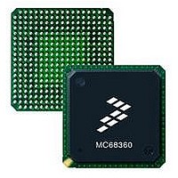
MC68EN360CAI25L Freescale Semiconductor, MC68EN360CAI25L Datasheet - Page 449

MC68EN360CAI25L
Manufacturer Part Number
MC68EN360CAI25L
Description
IC MPU QUICC 25MHZ 240-FQFP
Manufacturer
Freescale Semiconductor
Series
MC68000r
Datasheets
1.MC68EN302AG20BT.pdf
(8 pages)
2.MC68EN360VR25L.pdf
(14 pages)
3.MC68EN360VR25L.pdf
(2 pages)
4.MC68EN360CAI25L.pdf
(962 pages)
Specifications of MC68EN360CAI25L
Processor Type
M683xx 32-Bit
Speed
25MHz
Voltage
5V
Mounting Type
Surface Mount
Package / Case
240-FQFP
Core Size
32 Bit
Cpu Speed
25MHz
Embedded Interface Type
SCP, TDM
Digital Ic Case Style
FQFP
No. Of Pins
240
Supply Voltage Range
4.75V To 5.25V
Rohs Compliant
Yes
Family Name
M68xxx
Device Core
ColdFire
Device Core Size
32b
Frequency (max)
25MHz
Instruction Set Architecture
RISC
Supply Voltage 1 (typ)
5V
Operating Supply Voltage (max)
5.25V
Operating Supply Voltage (min)
4.75V
Operating Temp Range
-40C to 85C
Operating Temperature Classification
Industrial
Mounting
Surface Mount
Pin Count
240
Package Type
FQFP
Lead Free Status / RoHS Status
Lead free / RoHS Compliant
Features
-
Lead Free Status / Rohs Status
Compliant
Available stocks
Company
Part Number
Manufacturer
Quantity
Price
Company:
Part Number:
MC68EN360CAI25L
Manufacturer:
APLHA
Quantity:
12 000
Company:
Part Number:
MC68EN360CAI25L
Manufacturer:
Freescale Semiconductor
Quantity:
10 000
Part Number:
MC68EN360CAI25L
Manufacturer:
FREESCALE
Quantity:
20 000
- MC68EN302AG20BT PDF datasheet
- MC68EN360VR25L PDF datasheet #2
- MC68EN360VR25L PDF datasheet #3
- MC68EN360CAI25L PDF datasheet #4
- Current page: 449 of 962
- Download datasheet (4Mb)
7.10.7.1 BD TABLE POINTER (RBASE, TBASE). The RBASE and TBASE entries define
the starting location in the dual-port RAM for the set of BDs for receive and transmit func-
tions of the SCC. This provides a great deal of flexibility in how BDs for an SCC are parti-
tioned. By selecting RBASE and TBASE entries for all SCCs, and by setting the W-bit in the
last BD in each BD list, the user may select how many BDs to allocate for the transmit and
receive side of every SCC. The user must initialize these entries before enabling the corre-
sponding channel. Furthermore, the user should not configure BD tables of two enabled
SCCs to overlap, or erratic operation will occur.
7.10.7.2 SCC FUNCTION CODE REGISTERS (RFCR, TFCR). There are eight separate
function code registers for the four SCC channels: four for receive data buffers (RFCRx) and
four for transmit data buffers (TFCRx). The FC entry contains the value that the user would
like to appear on the function code pins FC3–FC0 when the associated SDMA channel
accesses memory. It also controls the byte-ordering convention to be used in the transfers.
Receive Function Code Register
NOTE: The items in boldface should be initialized by the user.
SCC Base + 0C
SCC Base + 1C
SCC Base + 2C
SCC Base + 00
SCC Base + 02
SCC Base + 04
SCC Base + 05
SCC Base + 06
SCC Base + 08
SCC Base + 10
SCC Base + 12
SCC Base + 14
SCC Base + 18
SCC Base + 20
SCC Base + 22
SCC Base + 24
SCC Base + 28
SCC Base + 30
SCC Base + xx
Address
RBASE and TBASE should contain a value that is divisible by 8.
Table 7-5. SCC Parameter RAM Common to All Protocols
Freescale Semiconductor, Inc.
7
For More Information On This Product,
RSTATE
TSTATE
MRBLR
RBASE
RBPTR
TBASE
TBPTR
RCRC
Name
RFCR
TFCR
TCRC
—
6
MC68360 USER’S MANUAL
Go to: www.freescale.com
5
MOT
NOTE
4
Width
Word
Word
Word
Word
Word
Word
Word
Long
Long
Long
Long
Long
Long
Long
Long
Byte
Byte
3
Serial Communication Controllers (SCCs)
2
FC3–FC0
Rx BD Base Address
Tx BD Base Address
Rx Function Code
Tx Function Code
Maximum Receive Buffer Length
Rx Internal State
Rx Internal Data Pointer
Rx BD Pointer
Rx Internal Byte Count
Rx Temp
Tx Internal State
Tx Internal Data Pointer
Tx BD Pointer
Tx Internal Byte Count
Tx Temp
Temp Receive CRC
Temp Transmit CRC
First Word of Protocol-Specific Area
Last Word of Protocol-Specific Area
1
Description
0
Related parts for MC68EN360CAI25L
Image
Part Number
Description
Manufacturer
Datasheet
Request
R
Part Number:
Description:
Manufacturer:
Freescale Semiconductor, Inc
Datasheet:
Part Number:
Description:
Manufacturer:
Freescale Semiconductor, Inc
Datasheet:
Part Number:
Description:
Manufacturer:
Freescale Semiconductor, Inc
Datasheet:
Part Number:
Description:
Manufacturer:
Freescale Semiconductor, Inc
Datasheet:
Part Number:
Description:
Manufacturer:
Freescale Semiconductor, Inc
Datasheet:
Part Number:
Description:
Manufacturer:
Freescale Semiconductor, Inc
Datasheet:
Part Number:
Description:
Manufacturer:
Freescale Semiconductor, Inc
Datasheet:
Part Number:
Description:
Manufacturer:
Freescale Semiconductor, Inc
Datasheet:
Part Number:
Description:
Manufacturer:
Freescale Semiconductor, Inc
Datasheet:
Part Number:
Description:
Manufacturer:
Freescale Semiconductor, Inc
Datasheet:
Part Number:
Description:
Manufacturer:
Freescale Semiconductor, Inc
Datasheet:
Part Number:
Description:
Manufacturer:
Freescale Semiconductor, Inc
Datasheet:
Part Number:
Description:
Manufacturer:
Freescale Semiconductor, Inc
Datasheet:
Part Number:
Description:
Manufacturer:
Freescale Semiconductor, Inc
Datasheet:
Part Number:
Description:
Manufacturer:
Freescale Semiconductor, Inc
Datasheet:


