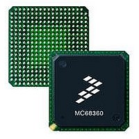
MC68EN360CAI25L Freescale Semiconductor, MC68EN360CAI25L Datasheet - Page 808

MC68EN360CAI25L
Manufacturer Part Number
MC68EN360CAI25L
Description
IC MPU QUICC 25MHZ 240-FQFP
Manufacturer
Freescale Semiconductor
Series
MC68000r
Datasheets
1.MC68EN302AG20BT.pdf
(8 pages)
2.MC68EN360VR25L.pdf
(14 pages)
3.MC68EN360VR25L.pdf
(2 pages)
4.MC68EN360CAI25L.pdf
(962 pages)
Specifications of MC68EN360CAI25L
Processor Type
M683xx 32-Bit
Speed
25MHz
Voltage
5V
Mounting Type
Surface Mount
Package / Case
240-FQFP
Core Size
32 Bit
Cpu Speed
25MHz
Embedded Interface Type
SCP, TDM
Digital Ic Case Style
FQFP
No. Of Pins
240
Supply Voltage Range
4.75V To 5.25V
Rohs Compliant
Yes
Family Name
M68xxx
Device Core
ColdFire
Device Core Size
32b
Frequency (max)
25MHz
Instruction Set Architecture
RISC
Supply Voltage 1 (typ)
5V
Operating Supply Voltage (max)
5.25V
Operating Supply Voltage (min)
4.75V
Operating Temp Range
-40C to 85C
Operating Temperature Classification
Industrial
Mounting
Surface Mount
Pin Count
240
Package Type
FQFP
Lead Free Status / RoHS Status
Lead free / RoHS Compliant
Features
-
Lead Free Status / Rohs Status
Compliant
Available stocks
Company
Part Number
Manufacturer
Quantity
Price
Company:
Part Number:
MC68EN360CAI25L
Manufacturer:
APLHA
Quantity:
12 000
Company:
Part Number:
MC68EN360CAI25L
Manufacturer:
Freescale Semiconductor
Quantity:
10 000
Part Number:
MC68EN360CAI25L
Manufacturer:
FREESCALE
Quantity:
20 000
- MC68EN302AG20BT PDF datasheet
- MC68EN360VR25L PDF datasheet #2
- MC68EN360VR25L PDF datasheet #3
- MC68EN360CAI25L PDF datasheet #4
- Current page: 808 of 962
- Download datasheet (4Mb)
Applications
The memory controller status register (MSTAT) is used for reporting write protect and parity
errors and does not require initialization.
The eight base registers (BRs), one for each memory bank, should be configured as follows:
The eight option registers (ORs), one for each memory bank, should be configured as fol-
lows:
9-88
one refresh every 15.6 s.
RFEN should be set.
RCYC depends on the DRAM speed. At 25 MHz (an 80-ns DRAM SIMM), RCYC should
be 00.
PGS2–PGS0 should be set to 011 for the 1M
DPS should be set to 00 (32-bit DRAM port size).
WBT40 does not apply to this application.
WBTQ depends on timing; it should be set for 80-ns MCM32100 SIMMs.
DWQ should be set if page mode enabled (PGME = 1).
DW40 does not apply to this application.
EMWS is not used in synchronous mode. (SYNC = 1)
SYNC should be set for a synchronous operation of the memory controller.
OPAR does not apply to this application.
PBEE does not apply to this application.
TSS40 does not apply to this application.
NCS should normally be cleared.
GAMX should be cleared for an external master system.
The BA27–BA11 bits may be set as desired. Different memory arrays should not overlap.
BA31–BA28 should be cleared since the byte write lines are used with an external master
in the system.
For simplicity, FC3–FC0 can be cleared.
TRLXQ depends on timing of memory/peripheral.
BACK40 does not apply to this application.
CSNT40 does not apply to this application.
CSNTQ should normally be cleared.
PAREN should be cleared since parity is not used in this application.
WP should be set for EPROM and flash EPROM; otherwise, it should be cleared.
V should be set if the memory bank is used.
The TCYC bits should be set to determine the number of wait states required.
Freescale Semiconductor, Inc.
For More Information On This Product,
MC68360 USER’S MANUAL
Go to: www.freescale.com
32 DRAM SIMM.
Related parts for MC68EN360CAI25L
Image
Part Number
Description
Manufacturer
Datasheet
Request
R
Part Number:
Description:
Manufacturer:
Freescale Semiconductor, Inc
Datasheet:
Part Number:
Description:
Manufacturer:
Freescale Semiconductor, Inc
Datasheet:
Part Number:
Description:
Manufacturer:
Freescale Semiconductor, Inc
Datasheet:
Part Number:
Description:
Manufacturer:
Freescale Semiconductor, Inc
Datasheet:
Part Number:
Description:
Manufacturer:
Freescale Semiconductor, Inc
Datasheet:
Part Number:
Description:
Manufacturer:
Freescale Semiconductor, Inc
Datasheet:
Part Number:
Description:
Manufacturer:
Freescale Semiconductor, Inc
Datasheet:
Part Number:
Description:
Manufacturer:
Freescale Semiconductor, Inc
Datasheet:
Part Number:
Description:
Manufacturer:
Freescale Semiconductor, Inc
Datasheet:
Part Number:
Description:
Manufacturer:
Freescale Semiconductor, Inc
Datasheet:
Part Number:
Description:
Manufacturer:
Freescale Semiconductor, Inc
Datasheet:
Part Number:
Description:
Manufacturer:
Freescale Semiconductor, Inc
Datasheet:
Part Number:
Description:
Manufacturer:
Freescale Semiconductor, Inc
Datasheet:
Part Number:
Description:
Manufacturer:
Freescale Semiconductor, Inc
Datasheet:
Part Number:
Description:
Manufacturer:
Freescale Semiconductor, Inc
Datasheet:


