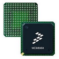
MC68EN360CAI25L Freescale Semiconductor, MC68EN360CAI25L Datasheet - Page 591

MC68EN360CAI25L
Manufacturer Part Number
MC68EN360CAI25L
Description
IC MPU QUICC 25MHZ 240-FQFP
Manufacturer
Freescale Semiconductor
Series
MC68000r
Datasheets
1.MC68EN302AG20BT.pdf
(8 pages)
2.MC68EN360VR25L.pdf
(14 pages)
3.MC68EN360VR25L.pdf
(2 pages)
4.MC68EN360CAI25L.pdf
(962 pages)
Specifications of MC68EN360CAI25L
Processor Type
M683xx 32-Bit
Speed
25MHz
Voltage
5V
Mounting Type
Surface Mount
Package / Case
240-FQFP
Core Size
32 Bit
Cpu Speed
25MHz
Embedded Interface Type
SCP, TDM
Digital Ic Case Style
FQFP
No. Of Pins
240
Supply Voltage Range
4.75V To 5.25V
Rohs Compliant
Yes
Family Name
M68xxx
Device Core
ColdFire
Device Core Size
32b
Frequency (max)
25MHz
Instruction Set Architecture
RISC
Supply Voltage 1 (typ)
5V
Operating Supply Voltage (max)
5.25V
Operating Supply Voltage (min)
4.75V
Operating Temp Range
-40C to 85C
Operating Temperature Classification
Industrial
Mounting
Surface Mount
Pin Count
240
Package Type
FQFP
Lead Free Status / RoHS Status
Lead free / RoHS Compliant
Features
-
Lead Free Status / Rohs Status
Compliant
Available stocks
Company
Part Number
Manufacturer
Quantity
Price
Company:
Part Number:
MC68EN360CAI25L
Manufacturer:
APLHA
Quantity:
12 000
Company:
Part Number:
MC68EN360CAI25L
Manufacturer:
Freescale Semiconductor
Quantity:
10 000
Part Number:
MC68EN360CAI25L
Manufacturer:
FREESCALE
Quantity:
20 000
- MC68EN302AG20BT PDF datasheet
- MC68EN360VR25L PDF datasheet #2
- MC68EN360VR25L PDF datasheet #3
- MC68EN360CAI25L PDF datasheet #4
- Current page: 591 of 962
- Download datasheet (4Mb)
After 14 bytes and the 46 bytes of automatic pad (plus the 4 bytes of CRC) have been trans-
mitted, the Tx BD is closed. Additionally, the receive buffer is closed after a frame is re-
ceived. Any additional receive data beyond 1520 bytes or a single frame will cause a busy
(out-of-buffers) condition since only one Rx BD was prepared.
20. Clear GADDR1–GADDR4. The group hash table is not
21. Write PADDR1_H with $0000, PADDR1_M with $0000, and PADDR1_L
22. Write P_Per with $0000. It is not used.
23. Clear IADDR1–IADDR4. The individual hash table is not
24. Clear TADDR_H, TADDR_M, and TADDR_L for the sake of clarity.
25. Initialize the Rx BD. Assume the Rx data buffer is at $00001000 in main memory.
26. Initialize the Tx BD. Assume the Tx data frame is at $00002000 in main memory
27. Write $FFFF to the SCCE to clear any previous events.
28. Write $001A to the SCCM to enable the TXE, RXF, and TXB interrupts.
29. Write $40000000 to the CIMR to allow SCC1 to generate a system interrupt. (The
30. Write $00000000 to GSMR_H1 to enable normal operation of all modes.
31. Write $1088000C to GSMR_L1 to configure the CTS (CLSN) and CD (RENA) pins
32. Write $D555 to DSR
33. Set the PSMR1 to $0A0A to configure 32-bit CRC, promiscuous mode (receive all
34. Enable the TENA pin (RTS). Since the MODE bits in GSMR have been written
35. Write $1088003C to GSMR_L1 to enable the SCC1 transmitter and receiver. This
used.
with $0040 to configure the physical address.
used.
Write $B000 to Rx_BD_Status. Write $0000 to Rx_BD_Length (not required—
done for instructional purposes only). Write $00001000 to Rx_BD_Pointer.
and contains fourteen 8-bit characters (destination and source addresses plus
the type field). Write $FC00 to Tx_BD_Status. Add PAD to the frame and
generate a CRC. Write $000D to Tx_BD_Length. Write $00002000 to
Tx_BD_Pointer.
CICR should also be initialized.)
to automatically control transmission and reception (DIAG bits) and the Ethernet
mode. TCI is set to allow more setup time for the EEST to receive the QUICC’s
transmit data. TPL and TPP are set as required for Ethernet. The DPLL is not used
with Ethernet. Notice that the transmitter (ENT) and receiver (ENR) have not been
enabled yet.
frames), and begin searching for the start frame delimiter 22 bits after RENA.
to Ethernet, the TENA signal is low. Write PCPAR bit 0 with a one. Write
PCDIR bit 0 with a zero.
additional write ensures that the ENT and ENR bits will be enabled last.
Freescale Semiconductor, Inc.
For More Information On This Product,
MC68360 USER’S MANUAL
Go to: www.freescale.com
NOTE
Serial Communication Controllers (SCCs)
Related parts for MC68EN360CAI25L
Image
Part Number
Description
Manufacturer
Datasheet
Request
R
Part Number:
Description:
Manufacturer:
Freescale Semiconductor, Inc
Datasheet:
Part Number:
Description:
Manufacturer:
Freescale Semiconductor, Inc
Datasheet:
Part Number:
Description:
Manufacturer:
Freescale Semiconductor, Inc
Datasheet:
Part Number:
Description:
Manufacturer:
Freescale Semiconductor, Inc
Datasheet:
Part Number:
Description:
Manufacturer:
Freescale Semiconductor, Inc
Datasheet:
Part Number:
Description:
Manufacturer:
Freescale Semiconductor, Inc
Datasheet:
Part Number:
Description:
Manufacturer:
Freescale Semiconductor, Inc
Datasheet:
Part Number:
Description:
Manufacturer:
Freescale Semiconductor, Inc
Datasheet:
Part Number:
Description:
Manufacturer:
Freescale Semiconductor, Inc
Datasheet:
Part Number:
Description:
Manufacturer:
Freescale Semiconductor, Inc
Datasheet:
Part Number:
Description:
Manufacturer:
Freescale Semiconductor, Inc
Datasheet:
Part Number:
Description:
Manufacturer:
Freescale Semiconductor, Inc
Datasheet:
Part Number:
Description:
Manufacturer:
Freescale Semiconductor, Inc
Datasheet:
Part Number:
Description:
Manufacturer:
Freescale Semiconductor, Inc
Datasheet:
Part Number:
Description:
Manufacturer:
Freescale Semiconductor, Inc
Datasheet:


