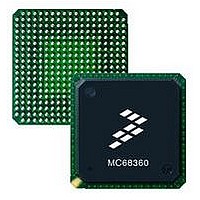
MC68EN360CAI25L Freescale Semiconductor, MC68EN360CAI25L Datasheet - Page 420

MC68EN360CAI25L
Manufacturer Part Number
MC68EN360CAI25L
Description
IC MPU QUICC 25MHZ 240-FQFP
Manufacturer
Freescale Semiconductor
Series
MC68000r
Datasheets
1.MC68EN302AG20BT.pdf
(8 pages)
2.MC68EN360VR25L.pdf
(14 pages)
3.MC68EN360VR25L.pdf
(2 pages)
4.MC68EN360CAI25L.pdf
(962 pages)
Specifications of MC68EN360CAI25L
Processor Type
M683xx 32-Bit
Speed
25MHz
Voltage
5V
Mounting Type
Surface Mount
Package / Case
240-FQFP
Core Size
32 Bit
Cpu Speed
25MHz
Embedded Interface Type
SCP, TDM
Digital Ic Case Style
FQFP
No. Of Pins
240
Supply Voltage Range
4.75V To 5.25V
Rohs Compliant
Yes
Family Name
M68xxx
Device Core
ColdFire
Device Core Size
32b
Frequency (max)
25MHz
Instruction Set Architecture
RISC
Supply Voltage 1 (typ)
5V
Operating Supply Voltage (max)
5.25V
Operating Supply Voltage (min)
4.75V
Operating Temp Range
-40C to 85C
Operating Temperature Classification
Industrial
Mounting
Surface Mount
Pin Count
240
Package Type
FQFP
Lead Free Status / RoHS Status
Lead free / RoHS Compliant
Features
-
Lead Free Status / Rohs Status
Compliant
Available stocks
Company
Part Number
Manufacturer
Quantity
Price
Company:
Part Number:
MC68EN360CAI25L
Manufacturer:
APLHA
Quantity:
12 000
Company:
Part Number:
MC68EN360CAI25L
Manufacturer:
Freescale Semiconductor
Quantity:
10 000
Part Number:
MC68EN360CAI25L
Manufacturer:
FREESCALE
Quantity:
20 000
- MC68EN302AG20BT PDF datasheet
- MC68EN360VR25L PDF datasheet #2
- MC68EN360VR25L PDF datasheet #3
- MC68EN360CAI25L PDF datasheet #4
- Current page: 420 of 962
- Download datasheet (4Mb)
Serial Interface with Time Slot Assigner
7.8.7 SI GCI Support
The normal mode of the GCI, also known as the ISDN-oriented modular rev 2.2 (IOM-2),
and the SCIT are fully supported by the QUICC. The QUICC also supports the D channel
access control in S/T interface terminals by using the command/indication (C/I) channel for
that function.
The GCI bus consists of four lines: two data lines, a clock, and a frame synchronization line.
Usually, an 8-kHz frame structure defines the various channels within the 256-kbps data
rate. The QUICC can support two independent GCI buses and has independent receive and
transmit sections for each one. The interface can also be used in a multiplexed frame struc-
ture on which up to eight physical layer devices multiplex their GCI channels. In this mode,
the data rate would be 2048 kbps.
In the GCI bus, the clock rate is twice the data rate. The SI divides the input clock by two to
produce the data clock.
The QUICC also has data strobe lines, and the 1 data rate clock L1CLKOx output pins.
These signals are used for interfacing devices to GCI that do not support the GCI bus.
The GCI signals for each transmit and receive channel are as follows:
7-96
5. PAPAR bits 6, 7, and 8 = 1. Configures L1TXDa, L1RXDa, and L1RCLKa.
6. PADIR bits 6 and 7 = 1. PADIR bit 8 = 0. Configures L1TXDa, L1RXDa, and
7. PCPAR bits 3, 10, and 11 = 1. Configures L1RQa, L1TSYNCa, and L1RSYNCa.
8. PCDIR bit 3 = 0. L1RQa is an input. L1TSYNCa will perform the L1GRa function
9. SIGMR = $04. Enable TDMa (one static TDM).
10. 1SICMR is not used.
11. 1SISTR and SIRP do not need to be read, but can be used for debugging
12. 1Enable the SCC1 for HDLC operation (to handle the LAPD protocol of
L1RSYNCx—Used as GCI sync signal; input to the QUICC. This signal indicates that
L1RCLKx—Used as GCI clock; input to the QUICC. The L1RCLKx signal is twice the
L1RXDx—Used as GCI receive data; input to the QUICC.
L1TXDx—Used as GCI transmit data; open-drain output. Valid only for the bits that are
L1CLKOx—Optional signal; output from QUICC. This 1 clock output can be used to
L1RCLKa.
and is therefore an output, but it does not need to be configured with a PCDIR bit.
L1RSYNCa is an input, but it does not need to be configured with a PCDIR bit.
information once the channels are enabled.
the D channel), and set SCC2 and SCC4 as desired.
the clock periods following the pulse designate the GCI frame.
data clock.
supported by the IDL; three-stated otherwise.
clock devices that do not interface directly to GCI. If the double-speed clock
Freescale Semiconductor, Inc.
For More Information On This Product,
MC68360 USER’S MANUAL
Go to: www.freescale.com
Related parts for MC68EN360CAI25L
Image
Part Number
Description
Manufacturer
Datasheet
Request
R
Part Number:
Description:
Manufacturer:
Freescale Semiconductor, Inc
Datasheet:
Part Number:
Description:
Manufacturer:
Freescale Semiconductor, Inc
Datasheet:
Part Number:
Description:
Manufacturer:
Freescale Semiconductor, Inc
Datasheet:
Part Number:
Description:
Manufacturer:
Freescale Semiconductor, Inc
Datasheet:
Part Number:
Description:
Manufacturer:
Freescale Semiconductor, Inc
Datasheet:
Part Number:
Description:
Manufacturer:
Freescale Semiconductor, Inc
Datasheet:
Part Number:
Description:
Manufacturer:
Freescale Semiconductor, Inc
Datasheet:
Part Number:
Description:
Manufacturer:
Freescale Semiconductor, Inc
Datasheet:
Part Number:
Description:
Manufacturer:
Freescale Semiconductor, Inc
Datasheet:
Part Number:
Description:
Manufacturer:
Freescale Semiconductor, Inc
Datasheet:
Part Number:
Description:
Manufacturer:
Freescale Semiconductor, Inc
Datasheet:
Part Number:
Description:
Manufacturer:
Freescale Semiconductor, Inc
Datasheet:
Part Number:
Description:
Manufacturer:
Freescale Semiconductor, Inc
Datasheet:
Part Number:
Description:
Manufacturer:
Freescale Semiconductor, Inc
Datasheet:
Part Number:
Description:
Manufacturer:
Freescale Semiconductor, Inc
Datasheet:


