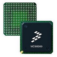
MC68EN360CAI25L Freescale Semiconductor, MC68EN360CAI25L Datasheet - Page 269

MC68EN360CAI25L
Manufacturer Part Number
MC68EN360CAI25L
Description
IC MPU QUICC 25MHZ 240-FQFP
Manufacturer
Freescale Semiconductor
Series
MC68000r
Datasheets
1.MC68EN302AG20BT.pdf
(8 pages)
2.MC68EN360VR25L.pdf
(14 pages)
3.MC68EN360VR25L.pdf
(2 pages)
4.MC68EN360CAI25L.pdf
(962 pages)
Specifications of MC68EN360CAI25L
Processor Type
M683xx 32-Bit
Speed
25MHz
Voltage
5V
Mounting Type
Surface Mount
Package / Case
240-FQFP
Core Size
32 Bit
Cpu Speed
25MHz
Embedded Interface Type
SCP, TDM
Digital Ic Case Style
FQFP
No. Of Pins
240
Supply Voltage Range
4.75V To 5.25V
Rohs Compliant
Yes
Family Name
M68xxx
Device Core
ColdFire
Device Core Size
32b
Frequency (max)
25MHz
Instruction Set Architecture
RISC
Supply Voltage 1 (typ)
5V
Operating Supply Voltage (max)
5.25V
Operating Supply Voltage (min)
4.75V
Operating Temp Range
-40C to 85C
Operating Temperature Classification
Industrial
Mounting
Surface Mount
Pin Count
240
Package Type
FQFP
Lead Free Status / RoHS Status
Lead free / RoHS Compliant
Features
-
Lead Free Status / Rohs Status
Compliant
Available stocks
Company
Part Number
Manufacturer
Quantity
Price
Company:
Part Number:
MC68EN360CAI25L
Manufacturer:
APLHA
Quantity:
12 000
Company:
Part Number:
MC68EN360CAI25L
Manufacturer:
Freescale Semiconductor
Quantity:
10 000
Part Number:
MC68EN360CAI25L
Manufacturer:
FREESCALE
Quantity:
20 000
- MC68EN302AG20BT PDF datasheet
- MC68EN360VR25L PDF datasheet #2
- MC68EN360VR25L PDF datasheet #3
- MC68EN360CAI25L PDF datasheet #4
- Current page: 269 of 962
- Download datasheet (4Mb)
The keyed write uses the MBAR enable (MBARE) register at address $0003FF08 and the
MBARE pin. Both the newly located MBAR and the MBARE are located in the CPU address
space FC = 111.
With multiple QUICCs configured in slave mode, the following keyed write is used to enable
the MBAR programming: the user writes the MBAR select bit of MBARE with a 1 while the
MBARE pin is a logic zero. Once this is accomplished, the MBAR may be written at its new
location (using the standard MBAR writing techniques). Once MBAR is written (in particular,
the low-order byte of MBAR), then the MBAR select bit in MBARE is cleared, and further
accesses to MBAR are impossible until the keyed write technique is used again. There is no
time limit imposed between the keyed write and the MBAR write; however, once the keyed
write for a particular QUICC slave has occurred, the MBAR of that slave should be written
before performing another keyed write to another QUICC slave.
The keyed write may be performed gluelessly to multiple QUICC slaves in the following way.
Connect (in hardware) the MBARE pin of QUICC slave #1 to bit zero of the data bus(D0).
Connect the MBARE pin of QUICC slave #2 to D1, etc. Then perform the following opera-
tions in software:
This technique will work for up to 31 QUICC slaves in the system, using no glue or parallel
I/O pins.
6.8.2 Global Chip Select (CS0) in Slave Mode
When the QUICC is in slave mode, the user may choose whether to enable the global chip-
select operation of CS0. (The global chip select is used for boot ROMs and is described in
6.10 Memory Controller.) The global chip select can be either enabled or disabled by the
configuration on the CONFIG pins during power-up reset and system reset (RESETH
asserted). When the global chip select function is disabled, CS0 can still be enabled later
and used as a normal chip select, if desired.
6.8.3 Bus Clear in Slave Mode
The bus clear out (BCLRO) pin can be selected to signify to the external logic that the DRAM
refresh controller, IDMA channels, or SDMA channels are requesting the bus. However, in
slave mode, the BCLRO pin may become the RAS2DD double drive pin, and a new pin
called bus clear in (BCLRI) is defined (at another location in the pinout). BCLRI indicates to
that QUICC that a request is being made for the QUICC to release the system bus. The EBI
will then clear all internal bus masters with an arbitration ID smaller than the programmed
value of the bus clear in ID (BCLRIID) in the MCR.
1. Write the MBARE of QUICC slave #1 at $0003FF08 with value $FFFFFFFE. This sets
2. Now the MBAR of QUICC slave #1 can be accessed at $0003FF04 and written using
3. Write the MBARE of QUICC slave #2 with the value $FFFFFFFD.
4. Now the MBAR of QUICC slave #2 can be written.
the MBAR select bit (bit 31) and places a low voltage on only the MBARE pin of QUICC
slave #1.
normal MBAR writing procedures.
Freescale Semiconductor, Inc.
For More Information On This Product,
MC68360 USER’S MANUAL
Go to: www.freescale.com
System Integration Module (SIM60)
Related parts for MC68EN360CAI25L
Image
Part Number
Description
Manufacturer
Datasheet
Request
R
Part Number:
Description:
Manufacturer:
Freescale Semiconductor, Inc
Datasheet:
Part Number:
Description:
Manufacturer:
Freescale Semiconductor, Inc
Datasheet:
Part Number:
Description:
Manufacturer:
Freescale Semiconductor, Inc
Datasheet:
Part Number:
Description:
Manufacturer:
Freescale Semiconductor, Inc
Datasheet:
Part Number:
Description:
Manufacturer:
Freescale Semiconductor, Inc
Datasheet:
Part Number:
Description:
Manufacturer:
Freescale Semiconductor, Inc
Datasheet:
Part Number:
Description:
Manufacturer:
Freescale Semiconductor, Inc
Datasheet:
Part Number:
Description:
Manufacturer:
Freescale Semiconductor, Inc
Datasheet:
Part Number:
Description:
Manufacturer:
Freescale Semiconductor, Inc
Datasheet:
Part Number:
Description:
Manufacturer:
Freescale Semiconductor, Inc
Datasheet:
Part Number:
Description:
Manufacturer:
Freescale Semiconductor, Inc
Datasheet:
Part Number:
Description:
Manufacturer:
Freescale Semiconductor, Inc
Datasheet:
Part Number:
Description:
Manufacturer:
Freescale Semiconductor, Inc
Datasheet:
Part Number:
Description:
Manufacturer:
Freescale Semiconductor, Inc
Datasheet:
Part Number:
Description:
Manufacturer:
Freescale Semiconductor, Inc
Datasheet:


