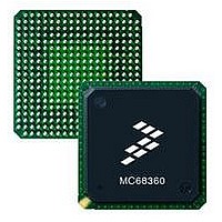
MC68EN360CAI25L Freescale Semiconductor, MC68EN360CAI25L Datasheet - Page 321

MC68EN360CAI25L
Manufacturer Part Number
MC68EN360CAI25L
Description
IC MPU QUICC 25MHZ 240-FQFP
Manufacturer
Freescale Semiconductor
Series
MC68000r
Datasheets
1.MC68EN302AG20BT.pdf
(8 pages)
2.MC68EN360VR25L.pdf
(14 pages)
3.MC68EN360VR25L.pdf
(2 pages)
4.MC68EN360CAI25L.pdf
(962 pages)
Specifications of MC68EN360CAI25L
Processor Type
M683xx 32-Bit
Speed
25MHz
Voltage
5V
Mounting Type
Surface Mount
Package / Case
240-FQFP
Core Size
32 Bit
Cpu Speed
25MHz
Embedded Interface Type
SCP, TDM
Digital Ic Case Style
FQFP
No. Of Pins
240
Supply Voltage Range
4.75V To 5.25V
Rohs Compliant
Yes
Family Name
M68xxx
Device Core
ColdFire
Device Core Size
32b
Frequency (max)
25MHz
Instruction Set Architecture
RISC
Supply Voltage 1 (typ)
5V
Operating Supply Voltage (max)
5.25V
Operating Supply Voltage (min)
4.75V
Operating Temp Range
-40C to 85C
Operating Temperature Classification
Industrial
Mounting
Surface Mount
Pin Count
240
Package Type
FQFP
Lead Free Status / RoHS Status
Lead free / RoHS Compliant
Features
-
Lead Free Status / Rohs Status
Compliant
Available stocks
Company
Part Number
Manufacturer
Quantity
Price
Company:
Part Number:
MC68EN360CAI25L
Manufacturer:
APLHA
Quantity:
12 000
Company:
Part Number:
MC68EN360CAI25L
Manufacturer:
Freescale Semiconductor
Quantity:
10 000
Part Number:
MC68EN360CAI25L
Manufacturer:
FREESCALE
Quantity:
20 000
- MC68EN302AG20BT PDF datasheet
- MC68EN360VR25L PDF datasheet #2
- MC68EN360VR25L PDF datasheet #3
- MC68EN360CAI25L PDF datasheet #4
- Current page: 321 of 962
- Download datasheet (4Mb)
TCYC3–TCYC0—Cycle Length in Clocks
This field determines the length of a bus cycle (see Table 6-14). Both internal masters and
external masters use this field for their accesses to a given memory bank. In addition, an
external MC68040 uses this field for the first access of a burst access sequence.
Although TCYC3–TCYC0 is the main parameter for determining cycle length since it se-
lects the number of wait states inserted in the cycle, the total cycle length may vary for
other reasons, such as a DRAM page hit, DRAM page miss, or whether the bus master
is internal or external to the QUICC. Besides TCYC, other bits that can affect the total cy-
cle length in certain situations are WBT40, WBTQ, DWQ, DW40, EMWS, SYNC, and
TSS40 in the GMR, and TRLXQ, PGME, and BCYC in the OR. CSNTQ and CSNT40 af-
fect the CS timing, but do not affect the total cycle length.
If the user has selected an external DSACKx or TA response for this memory bank, with
the SPS or DPS bits, then TCYC3–TCYC0 are not used.
TCYC =
15
…
0
1
2
3
4
5
6
If two chip selects are programmed to assert in the same ad-
dress region, only the lower chip select (or RAS line) will assert.
External cycles are always three clocks or longer. SeeTable 6-
11 for more details.
Normal DRAM cycles are three clocks when TCYC=0 and four
clocks when TCYC=1, etc. Therefore fast termination is not pos-
sible during the initial access to DRAM. Two clock DRAM cycles
are only possible when page mode is enabled for an internal
master.
If an external DSACK response is selected with either DPS in
the GMR or SPS in the OR, TCYC should not be set to zero.
For example, CS1 has priority over CS4.
Number
Number of Clocks
…
17
2
3
4
5
6
7
8
Freescale Semiconductor, Inc.
For More Information On This Product,
Table 6-14. Cycle Length in Clocks
Fast Termina-
Internal QUICC Master Memory Bus Cycle Length
Comments
Normal
MC68360 USER’S MANUAL
Go to: www.freescale.com
tion
NOTES
Number of Wait States
Number
…
14
0
1
2
3
4
5
*
(SRAM)
Comments
Undefined
System Integration Module (SIM60)
Number of Wait States
Numbers
(DRAM)
…
18
3
4
5
6
7
8
9
Related parts for MC68EN360CAI25L
Image
Part Number
Description
Manufacturer
Datasheet
Request
R
Part Number:
Description:
Manufacturer:
Freescale Semiconductor, Inc
Datasheet:
Part Number:
Description:
Manufacturer:
Freescale Semiconductor, Inc
Datasheet:
Part Number:
Description:
Manufacturer:
Freescale Semiconductor, Inc
Datasheet:
Part Number:
Description:
Manufacturer:
Freescale Semiconductor, Inc
Datasheet:
Part Number:
Description:
Manufacturer:
Freescale Semiconductor, Inc
Datasheet:
Part Number:
Description:
Manufacturer:
Freescale Semiconductor, Inc
Datasheet:
Part Number:
Description:
Manufacturer:
Freescale Semiconductor, Inc
Datasheet:
Part Number:
Description:
Manufacturer:
Freescale Semiconductor, Inc
Datasheet:
Part Number:
Description:
Manufacturer:
Freescale Semiconductor, Inc
Datasheet:
Part Number:
Description:
Manufacturer:
Freescale Semiconductor, Inc
Datasheet:
Part Number:
Description:
Manufacturer:
Freescale Semiconductor, Inc
Datasheet:
Part Number:
Description:
Manufacturer:
Freescale Semiconductor, Inc
Datasheet:
Part Number:
Description:
Manufacturer:
Freescale Semiconductor, Inc
Datasheet:
Part Number:
Description:
Manufacturer:
Freescale Semiconductor, Inc
Datasheet:
Part Number:
Description:
Manufacturer:
Freescale Semiconductor, Inc
Datasheet:


