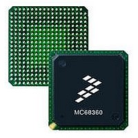
MC68EN360CAI25L Freescale Semiconductor, MC68EN360CAI25L Datasheet - Page 311

MC68EN360CAI25L
Manufacturer Part Number
MC68EN360CAI25L
Description
IC MPU QUICC 25MHZ 240-FQFP
Manufacturer
Freescale Semiconductor
Series
MC68000r
Datasheets
1.MC68EN302AG20BT.pdf
(8 pages)
2.MC68EN360VR25L.pdf
(14 pages)
3.MC68EN360VR25L.pdf
(2 pages)
4.MC68EN360CAI25L.pdf
(962 pages)
Specifications of MC68EN360CAI25L
Processor Type
M683xx 32-Bit
Speed
25MHz
Voltage
5V
Mounting Type
Surface Mount
Package / Case
240-FQFP
Core Size
32 Bit
Cpu Speed
25MHz
Embedded Interface Type
SCP, TDM
Digital Ic Case Style
FQFP
No. Of Pins
240
Supply Voltage Range
4.75V To 5.25V
Rohs Compliant
Yes
Family Name
M68xxx
Device Core
ColdFire
Device Core Size
32b
Frequency (max)
25MHz
Instruction Set Architecture
RISC
Supply Voltage 1 (typ)
5V
Operating Supply Voltage (max)
5.25V
Operating Supply Voltage (min)
4.75V
Operating Temp Range
-40C to 85C
Operating Temperature Classification
Industrial
Mounting
Surface Mount
Pin Count
240
Package Type
FQFP
Lead Free Status / RoHS Status
Lead free / RoHS Compliant
Features
-
Lead Free Status / Rohs Status
Compliant
Available stocks
Company
Part Number
Manufacturer
Quantity
Price
Company:
Part Number:
MC68EN360CAI25L
Manufacturer:
APLHA
Quantity:
12 000
Company:
Part Number:
MC68EN360CAI25L
Manufacturer:
Freescale Semiconductor
Quantity:
10 000
Part Number:
MC68EN360CAI25L
Manufacturer:
FREESCALE
Quantity:
20 000
- MC68EN302AG20BT PDF datasheet
- MC68EN360VR25L PDF datasheet #2
- MC68EN360VR25L PDF datasheet #3
- MC68EN360CAI25L PDF datasheet #4
- Current page: 311 of 962
- Download datasheet (4Mb)
EMWS—External Master Wait State (SRAM Bank Only)
The following bits are used for both DRAM and SRAM memory:
SYNC—Synchronous External Access MC68030-Type
This attribute should be set if an additional wait state is necessary when an asynchronous
external MC68030-type device or external QUICC is accessing SRAM banks (see Table
6-11). This bit is only used if SYNC = 0.
This attribute applies only to an external MC68030-type device or external QUICC that
uses the on-chip memory controller. It determines how the memory controller will assert
its signals in response to what it sees from the external master.
When the SRAM controller is used, CS and DSACK assertion and negation timings are
asynchronous. They are asserted and negated in relation to the external master’s AS line.
The CSNTQ and the TRLXQ attributes are ignored. When EMWS is set, one wait state is
added to the programmed TCYC.
When the DRAM controller is used, CAS and DSACK are negated asynchronously with
the negation of the external master’s AS.
0 = Normal operation.
1 = Insert one additional wait state for external QUICC/MC68030-type masters on their
0 = Asynchronous operation of the memory controller (external MC68030-type master
accesses to all SRAM banks.)
only).
chronous to the QUICC clock. When asynchronous external
masters are using the DRAM controller, the BSTM bit in the
MCR should be cleared.
The DRAM controller’s assertion of RAS and CAS is always syn-
0
1
2
3
4
5
6
15
NOTE: The BSTM bit is located in the MCR of the SI60.
TCYC =
Table 6-11. External MC68030-Type Cycle Length
…
(SRAM Bank in Asynchronous Operation
Freescale Semiconductor, Inc.
For More Information On This Product,
Synchronous Bus Timing
EMWS = 0
External QUICC/MC68030-Type Bus Cycle Length
17
…
3
3
4
5
6
7
8
MC68360 USER’S MANUAL
(BSTM = 1)
Go to: www.freescale.com
EMWS = 1
NOTE
18
…
3
4
5
6
7
8
9
Asynchronous Bus Timing
EMWS = 0
18
…
3
3
5
6
7
8
9
(BSTM = 0)
System Integration Module (SIM60)
EMWS = 1
10
19
…
3
5
6
7
8
9
Related parts for MC68EN360CAI25L
Image
Part Number
Description
Manufacturer
Datasheet
Request
R
Part Number:
Description:
Manufacturer:
Freescale Semiconductor, Inc
Datasheet:
Part Number:
Description:
Manufacturer:
Freescale Semiconductor, Inc
Datasheet:
Part Number:
Description:
Manufacturer:
Freescale Semiconductor, Inc
Datasheet:
Part Number:
Description:
Manufacturer:
Freescale Semiconductor, Inc
Datasheet:
Part Number:
Description:
Manufacturer:
Freescale Semiconductor, Inc
Datasheet:
Part Number:
Description:
Manufacturer:
Freescale Semiconductor, Inc
Datasheet:
Part Number:
Description:
Manufacturer:
Freescale Semiconductor, Inc
Datasheet:
Part Number:
Description:
Manufacturer:
Freescale Semiconductor, Inc
Datasheet:
Part Number:
Description:
Manufacturer:
Freescale Semiconductor, Inc
Datasheet:
Part Number:
Description:
Manufacturer:
Freescale Semiconductor, Inc
Datasheet:
Part Number:
Description:
Manufacturer:
Freescale Semiconductor, Inc
Datasheet:
Part Number:
Description:
Manufacturer:
Freescale Semiconductor, Inc
Datasheet:
Part Number:
Description:
Manufacturer:
Freescale Semiconductor, Inc
Datasheet:
Part Number:
Description:
Manufacturer:
Freescale Semiconductor, Inc
Datasheet:
Part Number:
Description:
Manufacturer:
Freescale Semiconductor, Inc
Datasheet:


