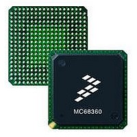
MC68EN360CAI25L Freescale Semiconductor, MC68EN360CAI25L Datasheet - Page 370

MC68EN360CAI25L
Manufacturer Part Number
MC68EN360CAI25L
Description
IC MPU QUICC 25MHZ 240-FQFP
Manufacturer
Freescale Semiconductor
Series
MC68000r
Datasheets
1.MC68EN302AG20BT.pdf
(8 pages)
2.MC68EN360VR25L.pdf
(14 pages)
3.MC68EN360VR25L.pdf
(2 pages)
4.MC68EN360CAI25L.pdf
(962 pages)
Specifications of MC68EN360CAI25L
Processor Type
M683xx 32-Bit
Speed
25MHz
Voltage
5V
Mounting Type
Surface Mount
Package / Case
240-FQFP
Core Size
32 Bit
Cpu Speed
25MHz
Embedded Interface Type
SCP, TDM
Digital Ic Case Style
FQFP
No. Of Pins
240
Supply Voltage Range
4.75V To 5.25V
Rohs Compliant
Yes
Family Name
M68xxx
Device Core
ColdFire
Device Core Size
32b
Frequency (max)
25MHz
Instruction Set Architecture
RISC
Supply Voltage 1 (typ)
5V
Operating Supply Voltage (max)
5.25V
Operating Supply Voltage (min)
4.75V
Operating Temp Range
-40C to 85C
Operating Temperature Classification
Industrial
Mounting
Surface Mount
Pin Count
240
Package Type
FQFP
Lead Free Status / RoHS Status
Lead free / RoHS Compliant
Features
-
Lead Free Status / Rohs Status
Compliant
Available stocks
Company
Part Number
Manufacturer
Quantity
Price
Company:
Part Number:
MC68EN360CAI25L
Manufacturer:
APLHA
Quantity:
12 000
Company:
Part Number:
MC68EN360CAI25L
Manufacturer:
Freescale Semiconductor
Quantity:
10 000
Part Number:
MC68EN360CAI25L
Manufacturer:
FREESCALE
Quantity:
20 000
- MC68EN302AG20BT PDF datasheet
- MC68EN360VR25L PDF datasheet #2
- MC68EN360VR25L PDF datasheet #3
- MC68EN360CAI25L PDF datasheet #4
- Current page: 370 of 962
- Download datasheet (4Mb)
IDMA Channels
Dual Address Destination Write . During this type of IDMA cycle, the data in the DHR is
written to the device or memory selected by the address in the DAPR, the destination func-
tion codes in the FCR, and the size in the CMR. The same options exist for operand size
and alignment as in the dual address source read. When the complete operand is written,
the DAPR is incremented by 1, 2, or 4, according to the DAPI and DSIZE bits of the CMR,
and the BTC is decremented by the number of bytes transferred. If the BTC is equal to zero,
the DONEx signal for the IDMA handshake is asserted, and if the transfer is completed with
no errors, the DONE bit in the CSR is set. See 7.5.2.4 Timer Reference Registers (TRR1,
TRR2, TRR3, TRR4) and 7.6.2.6 Byte Count Register (BCR) for more information.
Dual Address Packing . When dual address mode is selected, the IDMA can perform pack-
ing. Regardless of the source size, destination size, source starting address, or destination
starting address, the IDMA will use the most efficient packing algorithm possible to perform
the transfer in the fewest possible number of bus cycles.
Three examples of the packing technique follow.
Example 1. This simple example shows how packing is performed when the source and des-
tination sizes are the same—word. The source address is $00000001, and the destination
address is $20000000. The number of bytes to be transferred is 4.
IDMA channel 1 initialization required for this example:
7-46
—ICCR = $0720. Recommended normal configuration.
—FCR1 = $89. Source function code is 1000; destination function code is 1001.
—SAPR1 = $00000001. Source address.
—DAPR1 = $20000000. Destination address.
—BCR1 = $00000003. Byte transfer count.
The packing algorithms are subject to the restriction that the
IDMA never performs 3-byte transfers.
Figure 7-13. Dual Address Transfer Example
Freescale Semiconductor, Inc.
QUICC
IDMA
For More Information On This Product,
DHR
MC68360 USER’S MANUAL
Go to: www.freescale.com
DACKx
ADDR.
ADDR.
AND
TWO BUS CYCLES
REQUIRED
NOTE
DATA
BUS
1
2
1
PERIPHERAL
MEMORY
Related parts for MC68EN360CAI25L
Image
Part Number
Description
Manufacturer
Datasheet
Request
R
Part Number:
Description:
Manufacturer:
Freescale Semiconductor, Inc
Datasheet:
Part Number:
Description:
Manufacturer:
Freescale Semiconductor, Inc
Datasheet:
Part Number:
Description:
Manufacturer:
Freescale Semiconductor, Inc
Datasheet:
Part Number:
Description:
Manufacturer:
Freescale Semiconductor, Inc
Datasheet:
Part Number:
Description:
Manufacturer:
Freescale Semiconductor, Inc
Datasheet:
Part Number:
Description:
Manufacturer:
Freescale Semiconductor, Inc
Datasheet:
Part Number:
Description:
Manufacturer:
Freescale Semiconductor, Inc
Datasheet:
Part Number:
Description:
Manufacturer:
Freescale Semiconductor, Inc
Datasheet:
Part Number:
Description:
Manufacturer:
Freescale Semiconductor, Inc
Datasheet:
Part Number:
Description:
Manufacturer:
Freescale Semiconductor, Inc
Datasheet:
Part Number:
Description:
Manufacturer:
Freescale Semiconductor, Inc
Datasheet:
Part Number:
Description:
Manufacturer:
Freescale Semiconductor, Inc
Datasheet:
Part Number:
Description:
Manufacturer:
Freescale Semiconductor, Inc
Datasheet:
Part Number:
Description:
Manufacturer:
Freescale Semiconductor, Inc
Datasheet:
Part Number:
Description:
Manufacturer:
Freescale Semiconductor, Inc
Datasheet:


