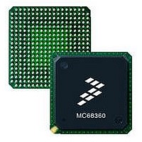
MC68EN360CAI25L Freescale Semiconductor, MC68EN360CAI25L Datasheet - Page 641

MC68EN360CAI25L
Manufacturer Part Number
MC68EN360CAI25L
Description
IC MPU QUICC 25MHZ 240-FQFP
Manufacturer
Freescale Semiconductor
Series
MC68000r
Datasheets
1.MC68EN302AG20BT.pdf
(8 pages)
2.MC68EN360VR25L.pdf
(14 pages)
3.MC68EN360VR25L.pdf
(2 pages)
4.MC68EN360CAI25L.pdf
(962 pages)
Specifications of MC68EN360CAI25L
Processor Type
M683xx 32-Bit
Speed
25MHz
Voltage
5V
Mounting Type
Surface Mount
Package / Case
240-FQFP
Core Size
32 Bit
Cpu Speed
25MHz
Embedded Interface Type
SCP, TDM
Digital Ic Case Style
FQFP
No. Of Pins
240
Supply Voltage Range
4.75V To 5.25V
Rohs Compliant
Yes
Family Name
M68xxx
Device Core
ColdFire
Device Core Size
32b
Frequency (max)
25MHz
Instruction Set Architecture
RISC
Supply Voltage 1 (typ)
5V
Operating Supply Voltage (max)
5.25V
Operating Supply Voltage (min)
4.75V
Operating Temp Range
-40C to 85C
Operating Temperature Classification
Industrial
Mounting
Surface Mount
Pin Count
240
Package Type
FQFP
Lead Free Status / RoHS Status
Lead free / RoHS Compliant
Features
-
Lead Free Status / Rohs Status
Compliant
Available stocks
Company
Part Number
Manufacturer
Quantity
Price
Company:
Part Number:
MC68EN360CAI25L
Manufacturer:
APLHA
Quantity:
12 000
Company:
Part Number:
MC68EN360CAI25L
Manufacturer:
Freescale Semiconductor
Quantity:
10 000
Part Number:
MC68EN360CAI25L
Manufacturer:
FREESCALE
Quantity:
20 000
- MC68EN302AG20BT PDF datasheet
- MC68EN360VR25L PDF datasheet #2
- MC68EN360VR25L PDF datasheet #3
- MC68EN360CAI25L PDF datasheet #4
- Current page: 641 of 962
- Download datasheet (4Mb)
7.12.5 SPI Programming Model
The following paragraphs describe the registers in the SPI.
7.12.5.1 SPI MODE REGISTER (SPMODE). SPMODE is a read-write register that controls
both the SPI operation mode and the SPI clock source. SPMODE is cleared by reset.
Bit 15—Reserved
LOOP—Loop Mode
CI—Clock Invert
CP—Clock Phase
DIV16—Divide by 16
REV—Reverse Data
15
This bit should be cleared by the user.
When set, this bit selects the local loopback operation. The transmitter output is internally
connected to the receiver input; the receiver and transmitter operate normally except that
the received data is ignored. (Loopback mode does not invert the SPI data, as do some
SPI-type devices such as the MC68302.)
The CI bit inverts the SPI clock polarity (refer to Figure 7-81 and Figure 7-82).
The CP bit selects one of two fundamentally different transfer formats (refer to Figure 7-
81 and Figure 7-82).
The DIV16 bit selects the clock source for the SPI baud rate generator when configured
as an SPI master. In slave mode, the clock source is the SPICLK pin.
The REV bit determines the receive and transmit character bit order.
—
0 = Normal operation.
1 = The SPI is in loopback mode.
0 = The inactive state of SPICLK is low.
1 = The inactive state of SPICLK is high.
0 = SPICLK begins toggling at the middle of the data transfer.
1 = SPICLK begins toggling at the beginning of the data transfer.
0 = Use the BRGCLK as the input to the SPI baud rate generator.
1 = Use the BRGCLK/16 as the input to the SPI baud rate generator.
0= Reverse data—LSB of character transmitted and received first.
1= Normal operation—MSB of character transmitted and received first.
LOOP
14
higher rates (6.25MHz in master mode and 12.5MHz in slave
mode). If multiple characters are to be transferred, a gap should
be inserted between transmission so that it will not exceed the
maximum data rate.
13
CI
CP
12
Freescale Semiconductor, Inc.
DIV16
11
For More Information On This Product,
REV
10
MC68360 USER’S MANUAL
Go to: www.freescale.com
M/S
9
EN
8
7
6
LEN
5
Serial Peripheral Interface (SPI)
4
PM3
3
PM2
2
PM1
1
PM0
0
Related parts for MC68EN360CAI25L
Image
Part Number
Description
Manufacturer
Datasheet
Request
R
Part Number:
Description:
Manufacturer:
Freescale Semiconductor, Inc
Datasheet:
Part Number:
Description:
Manufacturer:
Freescale Semiconductor, Inc
Datasheet:
Part Number:
Description:
Manufacturer:
Freescale Semiconductor, Inc
Datasheet:
Part Number:
Description:
Manufacturer:
Freescale Semiconductor, Inc
Datasheet:
Part Number:
Description:
Manufacturer:
Freescale Semiconductor, Inc
Datasheet:
Part Number:
Description:
Manufacturer:
Freescale Semiconductor, Inc
Datasheet:
Part Number:
Description:
Manufacturer:
Freescale Semiconductor, Inc
Datasheet:
Part Number:
Description:
Manufacturer:
Freescale Semiconductor, Inc
Datasheet:
Part Number:
Description:
Manufacturer:
Freescale Semiconductor, Inc
Datasheet:
Part Number:
Description:
Manufacturer:
Freescale Semiconductor, Inc
Datasheet:
Part Number:
Description:
Manufacturer:
Freescale Semiconductor, Inc
Datasheet:
Part Number:
Description:
Manufacturer:
Freescale Semiconductor, Inc
Datasheet:
Part Number:
Description:
Manufacturer:
Freescale Semiconductor, Inc
Datasheet:
Part Number:
Description:
Manufacturer:
Freescale Semiconductor, Inc
Datasheet:
Part Number:
Description:
Manufacturer:
Freescale Semiconductor, Inc
Datasheet:


