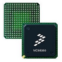
MC68EN360CAI25L Freescale Semiconductor, MC68EN360CAI25L Datasheet - Page 463

MC68EN360CAI25L
Manufacturer Part Number
MC68EN360CAI25L
Description
IC MPU QUICC 25MHZ 240-FQFP
Manufacturer
Freescale Semiconductor
Series
MC68000r
Datasheets
1.MC68EN302AG20BT.pdf
(8 pages)
2.MC68EN360VR25L.pdf
(14 pages)
3.MC68EN360VR25L.pdf
(2 pages)
4.MC68EN360CAI25L.pdf
(962 pages)
Specifications of MC68EN360CAI25L
Processor Type
M683xx 32-Bit
Speed
25MHz
Voltage
5V
Mounting Type
Surface Mount
Package / Case
240-FQFP
Core Size
32 Bit
Cpu Speed
25MHz
Embedded Interface Type
SCP, TDM
Digital Ic Case Style
FQFP
No. Of Pins
240
Supply Voltage Range
4.75V To 5.25V
Rohs Compliant
Yes
Family Name
M68xxx
Device Core
ColdFire
Device Core Size
32b
Frequency (max)
25MHz
Instruction Set Architecture
RISC
Supply Voltage 1 (typ)
5V
Operating Supply Voltage (max)
5.25V
Operating Supply Voltage (min)
4.75V
Operating Temp Range
-40C to 85C
Operating Temperature Classification
Industrial
Mounting
Surface Mount
Pin Count
240
Package Type
FQFP
Lead Free Status / RoHS Status
Lead free / RoHS Compliant
Features
-
Lead Free Status / Rohs Status
Compliant
Available stocks
Company
Part Number
Manufacturer
Quantity
Price
Company:
Part Number:
MC68EN360CAI25L
Manufacturer:
APLHA
Quantity:
12 000
Company:
Part Number:
MC68EN360CAI25L
Manufacturer:
Freescale Semiconductor
Quantity:
10 000
Part Number:
MC68EN360CAI25L
Manufacturer:
FREESCALE
Quantity:
20 000
- MC68EN302AG20BT PDF datasheet
- MC68EN360VR25L PDF datasheet #2
- MC68EN360VR25L PDF datasheet #3
- MC68EN360CAI25L PDF datasheet #4
- Current page: 463 of 962
- Download datasheet (4Mb)
7.10.13 Clock Glitch Detection
A clock glitch occurs when an input clock signal transitions between a one and zero state
twice, within a small enough time period to violate the minimum high/low time specification
of the input clock. Spikes are one type of glitch. Additionally, glitches can occur when exces-
sive noise is present on a slowly rising/falling signal.
Glitched clocks are a worry to many communications systems. Not only can they cause sys-
tems to experience errors, they can potentially cause errors to occur without even being
detected by the system. Systems that supply an external clock to a serial channel are often
susceptible to glitches from situations such as noise, connecting/disconnecting the physical
cable from the application board, or excessive ringing on the clock lines.
The SCCs on the QUICC have a special circuit designed to detect glitches that may occur
in the system. The glitch circuit is designed to detect glitches that could cause the SCC to
transition to the wrong state. This status information can be used to alert the system of a
problem at the physical layer.
The glitch detect circuit is not a specification test. Thus, if the user develops a circuit that
does not meet the input clocking specifications for the SCCs, erroneous data may be
received/transmitted that is not indicated by the glitch detection logic. Conversely, if a glitch
indication is signaled, it does not guarantee that erroneous data was received/transmitted.
Regardless of whether the DPLL is used, the received clock is passed through a noise filter
that eliminates any noise spikes that affect a single sample. This sampling is enabled with
the GDE bit of the GSMR.
If a spike is detected, a maskable receive or transmit glitched clock interrupt is generated in
the event register of the SCC channel. Although the user may choose to reset the SCC
receiver or transmitter or to continue operation, he should keep statistics on clock glitches
for later evaluation. In addition, the glitched status indication may be used as a debugging
aid during the early phases of prototype testing.
7.10.14 Disabling the SCCs on the Fly
If an SCC is not needed for a period of time, it may be disabled and reenabled later. In this
case, a sequence of operations is followed.
These sequences ensure that any buffers in use will be properly closed and that new data
will be transferred to/from a new buffer. Such a sequence is required if the parameters that
must be changed are not allowed to be changed dynamically. If the register or bit description
The 1:2 ratio of the SyncCLK to the serial clock does not apply
when the DPLL is used to recover the clock in the 8 , 16 , or 32
modes. The synchronization actually occurs internally after the
receive clock is generated by the DPLL; therefore, even the fast-
est DPLL clock generation (the 8 option) easily meets the re-
quired 1:2 ratio clocking limit.
Freescale Semiconductor, Inc.
For More Information On This Product,
MC68360 USER’S MANUAL
Go to: www.freescale.com
NOTE
Serial Communication Controllers (SCCs)
Related parts for MC68EN360CAI25L
Image
Part Number
Description
Manufacturer
Datasheet
Request
R
Part Number:
Description:
Manufacturer:
Freescale Semiconductor, Inc
Datasheet:
Part Number:
Description:
Manufacturer:
Freescale Semiconductor, Inc
Datasheet:
Part Number:
Description:
Manufacturer:
Freescale Semiconductor, Inc
Datasheet:
Part Number:
Description:
Manufacturer:
Freescale Semiconductor, Inc
Datasheet:
Part Number:
Description:
Manufacturer:
Freescale Semiconductor, Inc
Datasheet:
Part Number:
Description:
Manufacturer:
Freescale Semiconductor, Inc
Datasheet:
Part Number:
Description:
Manufacturer:
Freescale Semiconductor, Inc
Datasheet:
Part Number:
Description:
Manufacturer:
Freescale Semiconductor, Inc
Datasheet:
Part Number:
Description:
Manufacturer:
Freescale Semiconductor, Inc
Datasheet:
Part Number:
Description:
Manufacturer:
Freescale Semiconductor, Inc
Datasheet:
Part Number:
Description:
Manufacturer:
Freescale Semiconductor, Inc
Datasheet:
Part Number:
Description:
Manufacturer:
Freescale Semiconductor, Inc
Datasheet:
Part Number:
Description:
Manufacturer:
Freescale Semiconductor, Inc
Datasheet:
Part Number:
Description:
Manufacturer:
Freescale Semiconductor, Inc
Datasheet:
Part Number:
Description:
Manufacturer:
Freescale Semiconductor, Inc
Datasheet:


