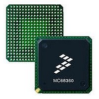
MC68EN360CAI25L Freescale Semiconductor, MC68EN360CAI25L Datasheet - Page 787

MC68EN360CAI25L
Manufacturer Part Number
MC68EN360CAI25L
Description
IC MPU QUICC 25MHZ 240-FQFP
Manufacturer
Freescale Semiconductor
Series
MC68000r
Datasheets
1.MC68EN302AG20BT.pdf
(8 pages)
2.MC68EN360VR25L.pdf
(14 pages)
3.MC68EN360VR25L.pdf
(2 pages)
4.MC68EN360CAI25L.pdf
(962 pages)
Specifications of MC68EN360CAI25L
Processor Type
M683xx 32-Bit
Speed
25MHz
Voltage
5V
Mounting Type
Surface Mount
Package / Case
240-FQFP
Core Size
32 Bit
Cpu Speed
25MHz
Embedded Interface Type
SCP, TDM
Digital Ic Case Style
FQFP
No. Of Pins
240
Supply Voltage Range
4.75V To 5.25V
Rohs Compliant
Yes
Family Name
M68xxx
Device Core
ColdFire
Device Core Size
32b
Frequency (max)
25MHz
Instruction Set Architecture
RISC
Supply Voltage 1 (typ)
5V
Operating Supply Voltage (max)
5.25V
Operating Supply Voltage (min)
4.75V
Operating Temp Range
-40C to 85C
Operating Temperature Classification
Industrial
Mounting
Surface Mount
Pin Count
240
Package Type
FQFP
Lead Free Status / RoHS Status
Lead free / RoHS Compliant
Features
-
Lead Free Status / Rohs Status
Compliant
Available stocks
Company
Part Number
Manufacturer
Quantity
Price
Company:
Part Number:
MC68EN360CAI25L
Manufacturer:
APLHA
Quantity:
12 000
Company:
Part Number:
MC68EN360CAI25L
Manufacturer:
Freescale Semiconductor
Quantity:
10 000
Part Number:
MC68EN360CAI25L
Manufacturer:
FREESCALE
Quantity:
20 000
- MC68EN302AG20BT PDF datasheet
- MC68EN360VR25L PDF datasheet #2
- MC68EN360VR25L PDF datasheet #3
- MC68EN360CAI25L PDF datasheet #4
- Current page: 787 of 962
- Download datasheet (4Mb)
Applications
The test logic is comprised of features that include the boundary scan register and is
accessed through the test access port (TAP).
9.7.1 Board Layout
The test equipment interfaces to the board through a test bus, with the tester acting as a test
bus master. This bus is comprised of the boundary scan signals and consists of one or sev-
eral parallel signal paths. Although different architectures are described in the JTAG stan-
dard document, this application shows only one serial connection. As shown in Figure 9-22,
one data signal loop is created with relevant device. The test data in (TDI) signal enters the
device and exits the device as test data out (TDO) at the other end of the shift register. In
addition, a clock signal (TCK) and a mode signal (TMS) are distributed to all devices in par-
allel.
An example of a board designed with the boundary scan path architecture is shown in Figure
9-22. Most devices, like device 2 through device 5, are included in the loop. Other devices
such as memories can be tested directly from a microprocessor. Usually, the board will also
contain small logic functions or analog ICs that do not contain boundary scan logic.
Once the board is tested with the test equipment, it is typically stored until it is installed in
the final system. This storage time is comprised of warehouse and shipping time. How then
can the board be retested before it begins to interact with a larger system in the end appli-
cation? This is of particular importance in telecommunication systems with distributed intel-
ligence, since an error can propagate throughout the entire system if one node is
malfunctioning.
Today, almost every board design includes some kind of processor or controller. This con-
troller can be used as the test bus master to perform a board test using an existing boundary
scan path. The following paragraphs describe how this concept can be achieved using the
QUICC as the board controller.
9-67
2. Testing of the device itself.
3. Observation or modification of the activity on the board.
Freescale Semiconductor, Inc.
For More Information On This Product,
MC68360 USER’S MANUAL
Go to: www.freescale.com
Related parts for MC68EN360CAI25L
Image
Part Number
Description
Manufacturer
Datasheet
Request
R
Part Number:
Description:
Manufacturer:
Freescale Semiconductor, Inc
Datasheet:
Part Number:
Description:
Manufacturer:
Freescale Semiconductor, Inc
Datasheet:
Part Number:
Description:
Manufacturer:
Freescale Semiconductor, Inc
Datasheet:
Part Number:
Description:
Manufacturer:
Freescale Semiconductor, Inc
Datasheet:
Part Number:
Description:
Manufacturer:
Freescale Semiconductor, Inc
Datasheet:
Part Number:
Description:
Manufacturer:
Freescale Semiconductor, Inc
Datasheet:
Part Number:
Description:
Manufacturer:
Freescale Semiconductor, Inc
Datasheet:
Part Number:
Description:
Manufacturer:
Freescale Semiconductor, Inc
Datasheet:
Part Number:
Description:
Manufacturer:
Freescale Semiconductor, Inc
Datasheet:
Part Number:
Description:
Manufacturer:
Freescale Semiconductor, Inc
Datasheet:
Part Number:
Description:
Manufacturer:
Freescale Semiconductor, Inc
Datasheet:
Part Number:
Description:
Manufacturer:
Freescale Semiconductor, Inc
Datasheet:
Part Number:
Description:
Manufacturer:
Freescale Semiconductor, Inc
Datasheet:
Part Number:
Description:
Manufacturer:
Freescale Semiconductor, Inc
Datasheet:
Part Number:
Description:
Manufacturer:
Freescale Semiconductor, Inc
Datasheet:


