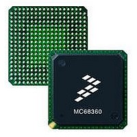
MC68EN360CAI25L Freescale Semiconductor, MC68EN360CAI25L Datasheet - Page 97

MC68EN360CAI25L
Manufacturer Part Number
MC68EN360CAI25L
Description
IC MPU QUICC 25MHZ 240-FQFP
Manufacturer
Freescale Semiconductor
Series
MC68000r
Datasheets
1.MC68EN302AG20BT.pdf
(8 pages)
2.MC68EN360VR25L.pdf
(14 pages)
3.MC68EN360VR25L.pdf
(2 pages)
4.MC68EN360CAI25L.pdf
(962 pages)
Specifications of MC68EN360CAI25L
Processor Type
M683xx 32-Bit
Speed
25MHz
Voltage
5V
Mounting Type
Surface Mount
Package / Case
240-FQFP
Core Size
32 Bit
Cpu Speed
25MHz
Embedded Interface Type
SCP, TDM
Digital Ic Case Style
FQFP
No. Of Pins
240
Supply Voltage Range
4.75V To 5.25V
Rohs Compliant
Yes
Family Name
M68xxx
Device Core
ColdFire
Device Core Size
32b
Frequency (max)
25MHz
Instruction Set Architecture
RISC
Supply Voltage 1 (typ)
5V
Operating Supply Voltage (max)
5.25V
Operating Supply Voltage (min)
4.75V
Operating Temp Range
-40C to 85C
Operating Temperature Classification
Industrial
Mounting
Surface Mount
Pin Count
240
Package Type
FQFP
Lead Free Status / RoHS Status
Lead free / RoHS Compliant
Features
-
Lead Free Status / Rohs Status
Compliant
Available stocks
Company
Part Number
Manufacturer
Quantity
Price
Company:
Part Number:
MC68EN360CAI25L
Manufacturer:
APLHA
Quantity:
12 000
Company:
Part Number:
MC68EN360CAI25L
Manufacturer:
Freescale Semiconductor
Quantity:
10 000
Part Number:
MC68EN360CAI25L
Manufacturer:
FREESCALE
Quantity:
20 000
- MC68EN302AG20BT PDF datasheet
- MC68EN360VR25L PDF datasheet #2
- MC68EN360VR25L PDF datasheet #3
- MC68EN360CAI25L PDF datasheet #4
- Current page: 97 of 962
- Download datasheet (4Mb)
Freescale Semiconductor, Inc.
Bus Operation
asserted in any asynchronous system. If this maximum delay time is violated, the QUICC
may exhibit erratic behavior.
4.2.5 Synchronous Operation with DSACKx
Although cycles terminated with DSACKx are classified as asynchronous, cycles terminated
with DSACKx can also operate synchronously in that signals are interpreted relative to clock
edges. The devices that use these cycles must synchronize the response to the QUICC
clock (CLKO1) to be synchronous. Since the devices terminate bus cycles with DSACKx,
the dynamic bus sizing capabilities of the QUICC are available. The minimum cycle time for
these cycles is also three clocks. To support systems that use the system clock to generate
DSACKx and other asynchronous inputs, the asynchronous input setup time and the asyn-
chronous input hold time are given. If the setup and hold times are met for the assertion or
negation of a signal, such as DSACKx, the QUICC is guaranteed to recognize that signal
level on that specific falling edge of the system clock. If the assertion of DSACKx is recog-
nized on a particular falling edge of the clock, valid data is latched into the QUICC (for a read
cycle) on the next falling clock edge if the data meets the data setup time. In this case, the
parameter for asynchronous operation can be ignored. The timing parameters are described
in Section 10 Electrical Characteristics.
If a system asserts DSACKx for the required window around the falling edge of S2 and
obeys the proper bus protocol by maintaining DSACKx (and/or BERR/HALT) until and
throughout the clock edge that negates AS (with the appropriate asynchronous input hold
time), no wait states are inserted. The bus cycle runs at its maximum speed for bus cycles
terminated with DSACKx (three clocks per cycle). When BERR (or BERR and HALT) is
asserted after DSACKx, BERR (and HALT) must meet the appropriate setup time prior to
the falling clock edge one clock cycle after DSACKx is recognized. This setup time is critical,
and the QUICC may exhibit erratic behavior if it is violated. When operating synchronously,
the data-in setup and hold times for synchronous cycles may be used instead of the timing
requirements for data relative to DS.
4.2.6 Fast Termination Cycles
With an external device that has a fast access time, the memory controller circuits can pro-
vide a two-clock external bus transfer. Since the memory controller circuits are driven from
the system clock, the bus cycle termination is inherently synchronized with the system clock.
Refer to Section 6 System Integration Module (SIM60) for more information on chip selects
and the DRAM controller. To use the fast termination (cycle length is two clocks) option, an
external device should be fast enough to have data ready, within the specified setup time,
by the falling edge of S4. Figure 4-14 shows the DSACKx timing for a read with two wait
states, followed by a fast termination read and write.
MC68360 USER’S MANUAL
For More Information On This Product,
Go to: www.freescale.com
Related parts for MC68EN360CAI25L
Image
Part Number
Description
Manufacturer
Datasheet
Request
R
Part Number:
Description:
Manufacturer:
Freescale Semiconductor, Inc
Datasheet:
Part Number:
Description:
Manufacturer:
Freescale Semiconductor, Inc
Datasheet:
Part Number:
Description:
Manufacturer:
Freescale Semiconductor, Inc
Datasheet:
Part Number:
Description:
Manufacturer:
Freescale Semiconductor, Inc
Datasheet:
Part Number:
Description:
Manufacturer:
Freescale Semiconductor, Inc
Datasheet:
Part Number:
Description:
Manufacturer:
Freescale Semiconductor, Inc
Datasheet:
Part Number:
Description:
Manufacturer:
Freescale Semiconductor, Inc
Datasheet:
Part Number:
Description:
Manufacturer:
Freescale Semiconductor, Inc
Datasheet:
Part Number:
Description:
Manufacturer:
Freescale Semiconductor, Inc
Datasheet:
Part Number:
Description:
Manufacturer:
Freescale Semiconductor, Inc
Datasheet:
Part Number:
Description:
Manufacturer:
Freescale Semiconductor, Inc
Datasheet:
Part Number:
Description:
Manufacturer:
Freescale Semiconductor, Inc
Datasheet:
Part Number:
Description:
Manufacturer:
Freescale Semiconductor, Inc
Datasheet:
Part Number:
Description:
Manufacturer:
Freescale Semiconductor, Inc
Datasheet:
Part Number:
Description:
Manufacturer:
Freescale Semiconductor, Inc
Datasheet:


