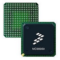
MC68EN360CAI25L Freescale Semiconductor, MC68EN360CAI25L Datasheet - Page 397

MC68EN360CAI25L
Manufacturer Part Number
MC68EN360CAI25L
Description
IC MPU QUICC 25MHZ 240-FQFP
Manufacturer
Freescale Semiconductor
Series
MC68000r
Datasheets
1.MC68EN302AG20BT.pdf
(8 pages)
2.MC68EN360VR25L.pdf
(14 pages)
3.MC68EN360VR25L.pdf
(2 pages)
4.MC68EN360CAI25L.pdf
(962 pages)
Specifications of MC68EN360CAI25L
Processor Type
M683xx 32-Bit
Speed
25MHz
Voltage
5V
Mounting Type
Surface Mount
Package / Case
240-FQFP
Core Size
32 Bit
Cpu Speed
25MHz
Embedded Interface Type
SCP, TDM
Digital Ic Case Style
FQFP
No. Of Pins
240
Supply Voltage Range
4.75V To 5.25V
Rohs Compliant
Yes
Family Name
M68xxx
Device Core
ColdFire
Device Core Size
32b
Frequency (max)
25MHz
Instruction Set Architecture
RISC
Supply Voltage 1 (typ)
5V
Operating Supply Voltage (max)
5.25V
Operating Supply Voltage (min)
4.75V
Operating Temp Range
-40C to 85C
Operating Temperature Classification
Industrial
Mounting
Surface Mount
Pin Count
240
Package Type
FQFP
Lead Free Status / RoHS Status
Lead free / RoHS Compliant
Features
-
Lead Free Status / Rohs Status
Compliant
Available stocks
Company
Part Number
Manufacturer
Quantity
Price
Company:
Part Number:
MC68EN360CAI25L
Manufacturer:
APLHA
Quantity:
12 000
Company:
Part Number:
MC68EN360CAI25L
Manufacturer:
Freescale Semiconductor
Quantity:
10 000
Part Number:
MC68EN360CAI25L
Manufacturer:
FREESCALE
Quantity:
20 000
- MC68EN302AG20BT PDF datasheet
- MC68EN360VR25L PDF datasheet #2
- MC68EN360VR25L PDF datasheet #3
- MC68EN360CAI25L PDF datasheet #4
- Current page: 397 of 962
- Download datasheet (4Mb)
SSEL1–SSEL4—Strobe Select
Bit 9—Reserved
The SWTR option gives station B the opportunity to listen to transmissions from station A
and to transmit data to Station A. To do this, station B would set the SWTR bit in its receive
route RAM. For this entry, receive data is taken from the L1TXD pin and data is transmit-
ted on the L1RXD pin. If the user only wants to listen to Station A’s transmissions and not
transmit data on L1RXD, then the CSEL bits in the corresponding transmit route RAM en-
try should be cleared to prevent transmission on the L1RXD pin.
It is also possible for station B to transmit data to station A by setting the SWTR bit of the
entry in its receive route RAM. Data is transmitted on the L1RXD pin rather than the
L1TXD pin, according to the transmit route RAM. Note that this configuration could cause
collisions with other data on the L1RXD pin unless care is taken to choose an available
(quiet) time slot. If the user only wants to transmit on L1RXD and not receive data on
L1TXD, then the CSEL bits in the receive route RAM should be cleared to prevent recep-
tion of data on L1TXD.
The four strobes (L1STA1, L1STA2, L1STB1, and L1STB2) may be assigned to the re-
ceive RAM and asserted/negated with L1RCLKa or L1RCLKb or assigned to the transmit
RAM and asserted/negated with L1TCLKa or L1TCLKb. Each bit corresponds to the value
the strobe should have during this bit/byte group. Multiple strobes can be asserted simul-
taneously, if desired.
If a strobe is configured to be asserted in two consecutive SI RAM entries, then it will re-
main continuously asserted during the processing of both SI RAM entries. If a strobe is
asserted on the last entry in the table, the strobe will be negated after the processing of
that last entry is complete.
0 = Normal operation of the L1TXD and L1RXD pins.
1 = Data is transmitted on the L1RXD pin and is received from the L1TXD pin for the
duration of this entry.
If the transmit and receive sections of the TDM do not use a sin-
gle clock source, this feature will give erratic results.
RX
STATION A
Freescale Semiconductor, Inc.
Figure 7-27. Using the SWTR Feature
For More Information On This Product,
TX
MC68360 USER’S MANUAL
Go to: www.freescale.com
RX
NOTE
STATION B
TX
Serial Interface with Time Slot Assigner
TDM TRANSMIT DATA
TDM RECEIVE DATA
Related parts for MC68EN360CAI25L
Image
Part Number
Description
Manufacturer
Datasheet
Request
R
Part Number:
Description:
Manufacturer:
Freescale Semiconductor, Inc
Datasheet:
Part Number:
Description:
Manufacturer:
Freescale Semiconductor, Inc
Datasheet:
Part Number:
Description:
Manufacturer:
Freescale Semiconductor, Inc
Datasheet:
Part Number:
Description:
Manufacturer:
Freescale Semiconductor, Inc
Datasheet:
Part Number:
Description:
Manufacturer:
Freescale Semiconductor, Inc
Datasheet:
Part Number:
Description:
Manufacturer:
Freescale Semiconductor, Inc
Datasheet:
Part Number:
Description:
Manufacturer:
Freescale Semiconductor, Inc
Datasheet:
Part Number:
Description:
Manufacturer:
Freescale Semiconductor, Inc
Datasheet:
Part Number:
Description:
Manufacturer:
Freescale Semiconductor, Inc
Datasheet:
Part Number:
Description:
Manufacturer:
Freescale Semiconductor, Inc
Datasheet:
Part Number:
Description:
Manufacturer:
Freescale Semiconductor, Inc
Datasheet:
Part Number:
Description:
Manufacturer:
Freescale Semiconductor, Inc
Datasheet:
Part Number:
Description:
Manufacturer:
Freescale Semiconductor, Inc
Datasheet:
Part Number:
Description:
Manufacturer:
Freescale Semiconductor, Inc
Datasheet:
Part Number:
Description:
Manufacturer:
Freescale Semiconductor, Inc
Datasheet:


