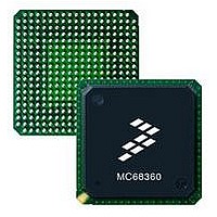
MC68EN360CAI25L Freescale Semiconductor, MC68EN360CAI25L Datasheet - Page 344

MC68EN360CAI25L
Manufacturer Part Number
MC68EN360CAI25L
Description
IC MPU QUICC 25MHZ 240-FQFP
Manufacturer
Freescale Semiconductor
Series
MC68000r
Datasheets
1.MC68EN302AG20BT.pdf
(8 pages)
2.MC68EN360VR25L.pdf
(14 pages)
3.MC68EN360VR25L.pdf
(2 pages)
4.MC68EN360CAI25L.pdf
(962 pages)
Specifications of MC68EN360CAI25L
Processor Type
M683xx 32-Bit
Speed
25MHz
Voltage
5V
Mounting Type
Surface Mount
Package / Case
240-FQFP
Core Size
32 Bit
Cpu Speed
25MHz
Embedded Interface Type
SCP, TDM
Digital Ic Case Style
FQFP
No. Of Pins
240
Supply Voltage Range
4.75V To 5.25V
Rohs Compliant
Yes
Family Name
M68xxx
Device Core
ColdFire
Device Core Size
32b
Frequency (max)
25MHz
Instruction Set Architecture
RISC
Supply Voltage 1 (typ)
5V
Operating Supply Voltage (max)
5.25V
Operating Supply Voltage (min)
4.75V
Operating Temp Range
-40C to 85C
Operating Temperature Classification
Industrial
Mounting
Surface Mount
Pin Count
240
Package Type
FQFP
Lead Free Status / RoHS Status
Lead free / RoHS Compliant
Features
-
Lead Free Status / Rohs Status
Compliant
Available stocks
Company
Part Number
Manufacturer
Quantity
Price
Company:
Part Number:
MC68EN360CAI25L
Manufacturer:
APLHA
Quantity:
12 000
Company:
Part Number:
MC68EN360CAI25L
Manufacturer:
Freescale Semiconductor
Quantity:
10 000
Part Number:
MC68EN360CAI25L
Manufacturer:
FREESCALE
Quantity:
20 000
- MC68EN302AG20BT PDF datasheet
- MC68EN360VR25L PDF datasheet #2
- MC68EN360VR25L PDF datasheet #3
- MC68EN360CAI25L PDF datasheet #4
- Current page: 344 of 962
- Download datasheet (4Mb)
Timers
When working in the cascaded mode, the cascaded TRR, TCR, and TCN should always be
referenced with 32-bit bus cycles.
7.5.2.2 TIMER GLOBAL CONFIGURATION REGISTER (TGCR). The TGCR is a 16-bit,
memory-mapped, read/write register that contains configuration parameters used by all four
timers. It allows starting and stopping any number of timers simultaneously if one bus cycle
is used to access TGCR. The TGCR is cleared by reset.
CAS4—Cascade Timers
CAS2—Cascade Timers
FRZ—Freeze
STP —Stop Timer
RST—Reset Timer
GM2—Gate Mode for Pin 2
7-20
CAS4
15
This bit is only valid if the gate function is enabled in TMR3 or TMR4.
0 = Normal Operation.
1 = Timers 3 and 4 are cascaded to form a 32-bit timer.
0 = Normal Operation.
1 = Timers 1 and 2 are cascaded to form a 32-bit timer.
0 = The corresponding timer ignores the FREEZE pin.
1 = Halt the corresponding timer if the FREEZE pin is asserted. (The FREEZE pin is
0 = Normal operation.
1 = Reduce power consumption of the timer. This bit stops all clocks to the timer, ex-
0 = Reset the corresponding timer (a software reset is identical to an external reset).
1 = Enable the corresponding timer if the STP bit is cleared.
0 = Restart gate mode. The TGATE2 pin is used to enable/disable the count. The fall-
1 = Normal gate mode. This mode is the same as 0, except the falling edge of TGATE2
FRZ4
14
asserted in background debug mode when the CPU32+ is enabled.)
cept the clock from the IMB interface, which allows the user to read and write timer
registers. The clocks to the timer remain stopped until the user clears this bit or a
hardware reset occurs.
ing edge of TGATE2 enables and restarts the count, and the rising edge of
TGATE2 disables the count.
does not restart the count value in TCN.
STP4
13
RST4
12
GM2
11
Freescale Semiconductor, Inc.
For More Information On This Product,
FRZ3
10
MC68360 USER’S MANUAL
Go to: www.freescale.com
STP3
9
RST3
8
CAS2
7
FRZ2
6
STP2
5
RST2
4
GM1
3
FRZ1
2
STP1
1
RST1
0
Related parts for MC68EN360CAI25L
Image
Part Number
Description
Manufacturer
Datasheet
Request
R
Part Number:
Description:
Manufacturer:
Freescale Semiconductor, Inc
Datasheet:
Part Number:
Description:
Manufacturer:
Freescale Semiconductor, Inc
Datasheet:
Part Number:
Description:
Manufacturer:
Freescale Semiconductor, Inc
Datasheet:
Part Number:
Description:
Manufacturer:
Freescale Semiconductor, Inc
Datasheet:
Part Number:
Description:
Manufacturer:
Freescale Semiconductor, Inc
Datasheet:
Part Number:
Description:
Manufacturer:
Freescale Semiconductor, Inc
Datasheet:
Part Number:
Description:
Manufacturer:
Freescale Semiconductor, Inc
Datasheet:
Part Number:
Description:
Manufacturer:
Freescale Semiconductor, Inc
Datasheet:
Part Number:
Description:
Manufacturer:
Freescale Semiconductor, Inc
Datasheet:
Part Number:
Description:
Manufacturer:
Freescale Semiconductor, Inc
Datasheet:
Part Number:
Description:
Manufacturer:
Freescale Semiconductor, Inc
Datasheet:
Part Number:
Description:
Manufacturer:
Freescale Semiconductor, Inc
Datasheet:
Part Number:
Description:
Manufacturer:
Freescale Semiconductor, Inc
Datasheet:
Part Number:
Description:
Manufacturer:
Freescale Semiconductor, Inc
Datasheet:
Part Number:
Description:
Manufacturer:
Freescale Semiconductor, Inc
Datasheet:


