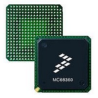
MC68EN360CAI25L Freescale Semiconductor, MC68EN360CAI25L Datasheet - Page 824

MC68EN360CAI25L
Manufacturer Part Number
MC68EN360CAI25L
Description
IC MPU QUICC 25MHZ 240-FQFP
Manufacturer
Freescale Semiconductor
Series
MC68000r
Datasheets
1.MC68EN302AG20BT.pdf
(8 pages)
2.MC68EN360VR25L.pdf
(14 pages)
3.MC68EN360VR25L.pdf
(2 pages)
4.MC68EN360CAI25L.pdf
(962 pages)
Specifications of MC68EN360CAI25L
Processor Type
M683xx 32-Bit
Speed
25MHz
Voltage
5V
Mounting Type
Surface Mount
Package / Case
240-FQFP
Core Size
32 Bit
Cpu Speed
25MHz
Embedded Interface Type
SCP, TDM
Digital Ic Case Style
FQFP
No. Of Pins
240
Supply Voltage Range
4.75V To 5.25V
Rohs Compliant
Yes
Family Name
M68xxx
Device Core
ColdFire
Device Core Size
32b
Frequency (max)
25MHz
Instruction Set Architecture
RISC
Supply Voltage 1 (typ)
5V
Operating Supply Voltage (max)
5.25V
Operating Supply Voltage (min)
4.75V
Operating Temp Range
-40C to 85C
Operating Temperature Classification
Industrial
Mounting
Surface Mount
Pin Count
240
Package Type
FQFP
Lead Free Status / RoHS Status
Lead free / RoHS Compliant
Features
-
Lead Free Status / Rohs Status
Compliant
Available stocks
Company
Part Number
Manufacturer
Quantity
Price
Company:
Part Number:
MC68EN360CAI25L
Manufacturer:
APLHA
Quantity:
12 000
Company:
Part Number:
MC68EN360CAI25L
Manufacturer:
Freescale Semiconductor
Quantity:
10 000
Part Number:
MC68EN360CAI25L
Manufacturer:
FREESCALE
Quantity:
20 000
- MC68EN302AG20BT PDF datasheet
- MC68EN360VR25L PDF datasheet #2
- MC68EN360VR25L PDF datasheet #3
- MC68EN360CAI25L PDF datasheet #4
- Current page: 824 of 962
- Download datasheet (4Mb)
Electrical Characteristics
10.9BUS OPERATION AC TIMING SPECIFICATIONS (CONTINUED
10-12
Num.
NOTES:
88
89
90
91
92
1. All AC timing is shown with respect to 0.8 V and 2.0 V levels unless otherwise noted.
2. This number can be reduced to 5 ns if strobes have equal loads.
3. If multiple chip selects are used, the CS¯ width negated (#15) applies to the time from the negation of a heavily load-
4. These hold times are specified with respect to DS or CS¯ on asynchronous reads and with respect to CLKO1 on fast
5. If the asynchronous setup time (#47) requirements are satisfied, the DSACK¯ low to data setup time (#31) and
6. To ensure coherency during every operand transfer, BG will not be asserted in response to BR until after cycles of
7. In the absence of DSACK¯ , BERR is an asynchronous input using the asynchronous setup time (#47).
8. During interrupt acknowledge cycles, the processor may insert up to two wait states between states S0 and S1.
9. These specs are for Synchronous Arbitration only. ASTM=1.
10.These CS¯ specs are for TRLX=0. If RAS¯ and RAS¯DD are connected together, reduce max value of RAS¯ spec-
11.These CS¯ specs are for TRLX=1. If RAS¯ and RAS¯DD are connected together, reduce max value of RAS¯ spec-
12.These CS¯ specs are for CSNTQ=0.
13.These CS¯ specs are for CSNTQ=1; or RAS¯ specs for DRAM accesses.
14.These specs are read cycles with parity check and PBEE=1.
15.These specs are read cycles with parity check and PBEE=0,PAREN=1.
16.These RAS¯ specs are for page miss case.
17. These specifications only apply to CS¯/RAS¯ pins.
18. This specification applies to non fast termination cycles. In fast termination cycles, the BERR signal must be negated
ed chip select to the assertion of a lightly loaded chip select.
termination reads. The user is free to use either hold time for fast termination reads.
DSACK¯ low to BERR low setup time (#48) can be ignored. The data must only satisfy the data-in to CLKO1 low
setup time (#27) for the following clock cycle: BERR must only satisfy the late BERR low to CLKO1 low setup time
(#27A) for the following clock cycle.
the current operand transfer are complete and RMC is negated.
ification by 1.5ns.
ification by 1.5ns.
by 20ns after negation of AS, DS.
CLKO1 High to IFETCH High Impedance
CLKO1 High to IFETCH Valid
CLKO1 High to PERR Asserted
CLKO1 High to PERR Negated
Minimum Vcc Ramp-Up Time At Power-On Reset
Characteristic
Freescale Semiconductor, Inc.
For More Information On This Product,
MC68360 USER’S MANUAL
Go to: www.freescale.com
Symbol
t CHPA
t CHPN
t RMIN
t IFZ
t IF
3.3 V/5.0 V
Min
25.0 MHz
0
0
5
0
0
Max
35
35
20
20
-
Min
0
0
0
0
5
33.34MHz
5.0V
26.25
26.25
Max
15
15
-
Unit
ms
ns
ns
ns
ns
Related parts for MC68EN360CAI25L
Image
Part Number
Description
Manufacturer
Datasheet
Request
R
Part Number:
Description:
Manufacturer:
Freescale Semiconductor, Inc
Datasheet:
Part Number:
Description:
Manufacturer:
Freescale Semiconductor, Inc
Datasheet:
Part Number:
Description:
Manufacturer:
Freescale Semiconductor, Inc
Datasheet:
Part Number:
Description:
Manufacturer:
Freescale Semiconductor, Inc
Datasheet:
Part Number:
Description:
Manufacturer:
Freescale Semiconductor, Inc
Datasheet:
Part Number:
Description:
Manufacturer:
Freescale Semiconductor, Inc
Datasheet:
Part Number:
Description:
Manufacturer:
Freescale Semiconductor, Inc
Datasheet:
Part Number:
Description:
Manufacturer:
Freescale Semiconductor, Inc
Datasheet:
Part Number:
Description:
Manufacturer:
Freescale Semiconductor, Inc
Datasheet:
Part Number:
Description:
Manufacturer:
Freescale Semiconductor, Inc
Datasheet:
Part Number:
Description:
Manufacturer:
Freescale Semiconductor, Inc
Datasheet:
Part Number:
Description:
Manufacturer:
Freescale Semiconductor, Inc
Datasheet:
Part Number:
Description:
Manufacturer:
Freescale Semiconductor, Inc
Datasheet:
Part Number:
Description:
Manufacturer:
Freescale Semiconductor, Inc
Datasheet:
Part Number:
Description:
Manufacturer:
Freescale Semiconductor, Inc
Datasheet:


