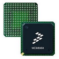
MC68EN360CAI25L Freescale Semiconductor, MC68EN360CAI25L Datasheet - Page 440

MC68EN360CAI25L
Manufacturer Part Number
MC68EN360CAI25L
Description
IC MPU QUICC 25MHZ 240-FQFP
Manufacturer
Freescale Semiconductor
Series
MC68000r
Datasheets
1.MC68EN302AG20BT.pdf
(8 pages)
2.MC68EN360VR25L.pdf
(14 pages)
3.MC68EN360VR25L.pdf
(2 pages)
4.MC68EN360CAI25L.pdf
(962 pages)
Specifications of MC68EN360CAI25L
Processor Type
M683xx 32-Bit
Speed
25MHz
Voltage
5V
Mounting Type
Surface Mount
Package / Case
240-FQFP
Core Size
32 Bit
Cpu Speed
25MHz
Embedded Interface Type
SCP, TDM
Digital Ic Case Style
FQFP
No. Of Pins
240
Supply Voltage Range
4.75V To 5.25V
Rohs Compliant
Yes
Family Name
M68xxx
Device Core
ColdFire
Device Core Size
32b
Frequency (max)
25MHz
Instruction Set Architecture
RISC
Supply Voltage 1 (typ)
5V
Operating Supply Voltage (max)
5.25V
Operating Supply Voltage (min)
4.75V
Operating Temp Range
-40C to 85C
Operating Temperature Classification
Industrial
Mounting
Surface Mount
Pin Count
240
Package Type
FQFP
Lead Free Status / RoHS Status
Lead free / RoHS Compliant
Features
-
Lead Free Status / Rohs Status
Compliant
Available stocks
Company
Part Number
Manufacturer
Quantity
Price
Company:
Part Number:
MC68EN360CAI25L
Manufacturer:
APLHA
Quantity:
12 000
Company:
Part Number:
MC68EN360CAI25L
Manufacturer:
Freescale Semiconductor
Quantity:
10 000
Part Number:
MC68EN360CAI25L
Manufacturer:
FREESCALE
Quantity:
20 000
- MC68EN302AG20BT PDF datasheet
- MC68EN360VR25L PDF datasheet #2
- MC68EN360VR25L PDF datasheet #3
- MC68EN360CAI25L PDF datasheet #4
- Current page: 440 of 962
- Download datasheet (4Mb)
Serial Communication Controllers (SCCs)
TCI—Transmit Clock Invert
TSNC—Transmit Sense
RINV—DPLL Receive Input Invert Data
TINV—DPLL Transmit Input Invert Data
7-116
This bit indicates the amount of time the internal sense signal will stay active after the last
transition on the RXD pin, indicating that the line is free. For instance, these bits can be
used in the AppleTalk protocol to avoid the spurious CS-changed interrupt that would oth-
erwise occur during the frame sync sequence that precedes the opening flags.
If RDCR is configured to 1 mode, the delay is the greater of the two numbers listed. If
RDCR is configured to 8 , 16 , or 32 mode, the delay is the lesser of the two numbers
listed.
0 = Normal operation.
1 = The internal transmit clock (TCLK) is inverted by the SCC before it is used. This
00 = Infinite—carrier sense is always active (default)
01 = 14 or 6.5 bit times as determined by the RDCR bits
10 = 4 or 1.5 bit times as determined by the RDCR bits (normally chosen for AppleTalk)
11 = 3 or 1 bit times as determined by the RDCR bits
0 = No invert
1 = Invert the data before it is sent to the on-chip DPLL for reception. This setting is
0 = No invert
1 = Invert the data before it is sent to the on-chip DPLL for transmission. This setting
option allows the SCC to clock data out one-half clock earlier, on the rising edge of
TCLK rather than the falling edge. In this mode, the SCC offers a minimum and
maximum "rising clock edge to data" specification. Data output by the SCC after
the rising edge of an external transmit clock can be latched by the external receiver
one clock cycle later on the next rising edge of the same transmit clock. This option
is recommended for Ethernet, HDLC, or transparent operation when the clock
rates are high (e.g., above 8 MHz) to improve data setup time for the external re-
ceiver.
used to produce FM1 from FM0, NRZI space from NRZI mark, etc. It may also be
used in regular NRZ mode to invert the data stream.
is used to produce FM1 from FM0, NRZI space from NRZI mark, etc. It may also
be used in regular NRZ mode to invert the data stream.
This bit must be 0 in HDLC BUS mode.
This bit must be 0 in HDLC BUS mode.
In T1 applications, setting TINV and TEND creates a continu-
ously inverted HDLC data stream.
Freescale Semiconductor, Inc.
For More Information On This Product,
MC68360 USER’S MANUAL
Go to: www.freescale.com
NOTE
NOTE
Related parts for MC68EN360CAI25L
Image
Part Number
Description
Manufacturer
Datasheet
Request
R
Part Number:
Description:
Manufacturer:
Freescale Semiconductor, Inc
Datasheet:
Part Number:
Description:
Manufacturer:
Freescale Semiconductor, Inc
Datasheet:
Part Number:
Description:
Manufacturer:
Freescale Semiconductor, Inc
Datasheet:
Part Number:
Description:
Manufacturer:
Freescale Semiconductor, Inc
Datasheet:
Part Number:
Description:
Manufacturer:
Freescale Semiconductor, Inc
Datasheet:
Part Number:
Description:
Manufacturer:
Freescale Semiconductor, Inc
Datasheet:
Part Number:
Description:
Manufacturer:
Freescale Semiconductor, Inc
Datasheet:
Part Number:
Description:
Manufacturer:
Freescale Semiconductor, Inc
Datasheet:
Part Number:
Description:
Manufacturer:
Freescale Semiconductor, Inc
Datasheet:
Part Number:
Description:
Manufacturer:
Freescale Semiconductor, Inc
Datasheet:
Part Number:
Description:
Manufacturer:
Freescale Semiconductor, Inc
Datasheet:
Part Number:
Description:
Manufacturer:
Freescale Semiconductor, Inc
Datasheet:
Part Number:
Description:
Manufacturer:
Freescale Semiconductor, Inc
Datasheet:
Part Number:
Description:
Manufacturer:
Freescale Semiconductor, Inc
Datasheet:
Part Number:
Description:
Manufacturer:
Freescale Semiconductor, Inc
Datasheet:


