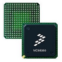
MC68EN360CAI25L Freescale Semiconductor, MC68EN360CAI25L Datasheet - Page 795

MC68EN360CAI25L
Manufacturer Part Number
MC68EN360CAI25L
Description
IC MPU QUICC 25MHZ 240-FQFP
Manufacturer
Freescale Semiconductor
Series
MC68000r
Datasheets
1.MC68EN302AG20BT.pdf
(8 pages)
2.MC68EN360VR25L.pdf
(14 pages)
3.MC68EN360VR25L.pdf
(2 pages)
4.MC68EN360CAI25L.pdf
(962 pages)
Specifications of MC68EN360CAI25L
Processor Type
M683xx 32-Bit
Speed
25MHz
Voltage
5V
Mounting Type
Surface Mount
Package / Case
240-FQFP
Core Size
32 Bit
Cpu Speed
25MHz
Embedded Interface Type
SCP, TDM
Digital Ic Case Style
FQFP
No. Of Pins
240
Supply Voltage Range
4.75V To 5.25V
Rohs Compliant
Yes
Family Name
M68xxx
Device Core
ColdFire
Device Core Size
32b
Frequency (max)
25MHz
Instruction Set Architecture
RISC
Supply Voltage 1 (typ)
5V
Operating Supply Voltage (max)
5.25V
Operating Supply Voltage (min)
4.75V
Operating Temp Range
-40C to 85C
Operating Temperature Classification
Industrial
Mounting
Surface Mount
Pin Count
240
Package Type
FQFP
Lead Free Status / RoHS Status
Lead free / RoHS Compliant
Features
-
Lead Free Status / Rohs Status
Compliant
Available stocks
Company
Part Number
Manufacturer
Quantity
Price
Company:
Part Number:
MC68EN360CAI25L
Manufacturer:
APLHA
Quantity:
12 000
Company:
Part Number:
MC68EN360CAI25L
Manufacturer:
Freescale Semiconductor
Quantity:
10 000
Part Number:
MC68EN360CAI25L
Manufacturer:
FREESCALE
Quantity:
20 000
- MC68EN302AG20BT PDF datasheet
- MC68EN360VR25L PDF datasheet #2
- MC68EN360VR25L PDF datasheet #3
- MC68EN360CAI25L PDF datasheet #4
- Current page: 795 of 962
- Download datasheet (4Mb)
Freescale Semiconductor, Inc.
Applications
9.8.1.1 MC68EC030 READS AND WRITES TO QUICC. The basic connection is made
through the data and address bus. All 32 data lines are routed between devices, which is
required for the connection. In slave mode, the QUICC is not allowed to use its 16-bit data
bus mode.(Assertion of 16BM pin during reset)
Twenty-eight address lines are routed between devices, giving a 256-Mbyte shared address
capability. It is possible to share all 32 address lines between devices, but the QUICC would
then lose its write enable lines (WE3–WE0). Since these lines are very useful in memory
interfaces, they are used in this application.
When running in normal slave mode with an MC68EC030 master, the QUICC provides a
few signal changes to support the MC68EC030. These signal changes allow the QUICC to
monitor and control the system buses in a glueless manner. The changed bus signals are
bus request (BR), bus grant (BG), and bus grant acknowledge (BGACK). When operating
in normal slave mode, the direction of these signals is reversed. Therefore, BR is an output;
BG is an input. In addition, BGACK becomes an I/O signal, rather than just an input.
9.8.1.2 CLOCKING STRATEGY. In this application, a single 25-MHz external oscillator is
used to drive the QUICC and the MC68EC030, which allows the synchronous mode of the
QUICC memory controller to be used. When considering buffering of outputs and board lay-
out, designers need to consider the synchronous timing requirements of the QUICC.
Designers considering the possibility of running asynchronously or with faster MC68EC030
clock speeds should reference paragraph 9.8.5 Using a Higher Speed MC68EC030 Master
with the QUICC.
9-75
MC68360 USER’S MANUAL
For More Information On This Product,
Go to: www.freescale.com
Related parts for MC68EN360CAI25L
Image
Part Number
Description
Manufacturer
Datasheet
Request
R
Part Number:
Description:
Manufacturer:
Freescale Semiconductor, Inc
Datasheet:
Part Number:
Description:
Manufacturer:
Freescale Semiconductor, Inc
Datasheet:
Part Number:
Description:
Manufacturer:
Freescale Semiconductor, Inc
Datasheet:
Part Number:
Description:
Manufacturer:
Freescale Semiconductor, Inc
Datasheet:
Part Number:
Description:
Manufacturer:
Freescale Semiconductor, Inc
Datasheet:
Part Number:
Description:
Manufacturer:
Freescale Semiconductor, Inc
Datasheet:
Part Number:
Description:
Manufacturer:
Freescale Semiconductor, Inc
Datasheet:
Part Number:
Description:
Manufacturer:
Freescale Semiconductor, Inc
Datasheet:
Part Number:
Description:
Manufacturer:
Freescale Semiconductor, Inc
Datasheet:
Part Number:
Description:
Manufacturer:
Freescale Semiconductor, Inc
Datasheet:
Part Number:
Description:
Manufacturer:
Freescale Semiconductor, Inc
Datasheet:
Part Number:
Description:
Manufacturer:
Freescale Semiconductor, Inc
Datasheet:
Part Number:
Description:
Manufacturer:
Freescale Semiconductor, Inc
Datasheet:
Part Number:
Description:
Manufacturer:
Freescale Semiconductor, Inc
Datasheet:
Part Number:
Description:
Manufacturer:
Freescale Semiconductor, Inc
Datasheet:


