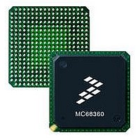
MC68EN360CAI25L Freescale Semiconductor, MC68EN360CAI25L Datasheet - Page 425

MC68EN360CAI25L
Manufacturer Part Number
MC68EN360CAI25L
Description
IC MPU QUICC 25MHZ 240-FQFP
Manufacturer
Freescale Semiconductor
Series
MC68000r
Datasheets
1.MC68EN302AG20BT.pdf
(8 pages)
2.MC68EN360VR25L.pdf
(14 pages)
3.MC68EN360VR25L.pdf
(2 pages)
4.MC68EN360CAI25L.pdf
(962 pages)
Specifications of MC68EN360CAI25L
Processor Type
M683xx 32-Bit
Speed
25MHz
Voltage
5V
Mounting Type
Surface Mount
Package / Case
240-FQFP
Core Size
32 Bit
Cpu Speed
25MHz
Embedded Interface Type
SCP, TDM
Digital Ic Case Style
FQFP
No. Of Pins
240
Supply Voltage Range
4.75V To 5.25V
Rohs Compliant
Yes
Family Name
M68xxx
Device Core
ColdFire
Device Core Size
32b
Frequency (max)
25MHz
Instruction Set Architecture
RISC
Supply Voltage 1 (typ)
5V
Operating Supply Voltage (max)
5.25V
Operating Supply Voltage (min)
4.75V
Operating Temp Range
-40C to 85C
Operating Temperature Classification
Industrial
Mounting
Surface Mount
Pin Count
240
Package Type
FQFP
Lead Free Status / RoHS Status
Lead free / RoHS Compliant
Features
-
Lead Free Status / Rohs Status
Compliant
Available stocks
Company
Part Number
Manufacturer
Quantity
Price
Company:
Part Number:
MC68EN360CAI25L
Manufacturer:
APLHA
Quantity:
12 000
Company:
Part Number:
MC68EN360CAI25L
Manufacturer:
Freescale Semiconductor
Quantity:
10 000
Part Number:
MC68EN360CAI25L
Manufacturer:
FREESCALE
Quantity:
20 000
- MC68EN302AG20BT PDF datasheet
- MC68EN360VR25L PDF datasheet #2
- MC68EN360VR25L PDF datasheet #3
- MC68EN360CAI25L PDF datasheet #4
- Current page: 425 of 962
- Download datasheet (4Mb)
choose its clock from a pre-defined pin or baud rate generator, which allows flexibility in the
pinout mapping strategy. Second, if a group of SCC receivers and transmitters need the
same clock rate, they can share the same pin. This configuration leaves additional pins for
other functions and minimizes potential skew between multiple clock sources.
The four baud rate generators also make their clocks available to external logic, regardless
of whether the baud rate generators are being used by an SCC or SMC. Note that the
BRGOx pins are multiplexed with other functions; therefore, all BRGOx pins may not always
be available. Note that BRGO3 has the flexibility to be output on both port A 12 and port B
16. See the pinout description in Section 11 Ordering Information and Mechanical Data for
more details.
There are a few restrictions in the bank-of-clocks mapping. First, only eight of the twelve
sources can be connected to any given SCC receiver or transmitter. Second the SMC trans-
mitter must have the same clock source as the receiver when connected to the NMSI pins.
Once the clock source is selected, the clock is given an internal name. For the SCCs, the
name is RCLKx and TCLKx. For the SMCs, the name is simply SMCLKx. These internal
names are used only in NMSI mode to specify the clock that is sent to the SCC or SMC.
These names do not correspond to any pins on the QUICC.
The exact pins available to each SCC and SMC in the NMSI mode are summarized in Figure
7-35.
The SCC1 in NMSI mode has its own set of modem control pins:
The SCC2 in NMSI mode has its own set of modem control pins:
TXD1
RXD1
TCLK1 <- BRG1–BRG4, CLK1–CLK4
RCLK1 <- BRG1–BRG4, CLK1–CLK4
RTS1
CTS1
CD1
TXD2
RXD2
TCLK2 <- BRG1–BRG4, CLK1–CLK4
RCLK2 <- BRG1–BRG4, CLK1–CLK4
RTS2
The internal RCLKx and TCLKx may be used as inputs to the
DPLL unit, which is inside the SCC. Thus, the RCLKx and
TCLKx signals are not required to always reflect the actual bit
rate on the line.
Freescale Semiconductor, Inc.
For More Information On This Product,
MC68360 USER’S MANUAL
Go to: www.freescale.com
NOTE
Serial Interface with Time Slot Assigner
Related parts for MC68EN360CAI25L
Image
Part Number
Description
Manufacturer
Datasheet
Request
R
Part Number:
Description:
Manufacturer:
Freescale Semiconductor, Inc
Datasheet:
Part Number:
Description:
Manufacturer:
Freescale Semiconductor, Inc
Datasheet:
Part Number:
Description:
Manufacturer:
Freescale Semiconductor, Inc
Datasheet:
Part Number:
Description:
Manufacturer:
Freescale Semiconductor, Inc
Datasheet:
Part Number:
Description:
Manufacturer:
Freescale Semiconductor, Inc
Datasheet:
Part Number:
Description:
Manufacturer:
Freescale Semiconductor, Inc
Datasheet:
Part Number:
Description:
Manufacturer:
Freescale Semiconductor, Inc
Datasheet:
Part Number:
Description:
Manufacturer:
Freescale Semiconductor, Inc
Datasheet:
Part Number:
Description:
Manufacturer:
Freescale Semiconductor, Inc
Datasheet:
Part Number:
Description:
Manufacturer:
Freescale Semiconductor, Inc
Datasheet:
Part Number:
Description:
Manufacturer:
Freescale Semiconductor, Inc
Datasheet:
Part Number:
Description:
Manufacturer:
Freescale Semiconductor, Inc
Datasheet:
Part Number:
Description:
Manufacturer:
Freescale Semiconductor, Inc
Datasheet:
Part Number:
Description:
Manufacturer:
Freescale Semiconductor, Inc
Datasheet:
Part Number:
Description:
Manufacturer:
Freescale Semiconductor, Inc
Datasheet:


