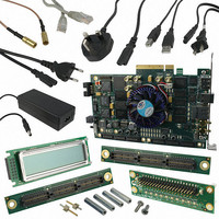
DK-DEV-4SGX230N Altera, DK-DEV-4SGX230N Datasheet - Page 1054

DK-DEV-4SGX230N
Manufacturer Part Number
DK-DEV-4SGX230N
Description
KIT DEVELOPMENT STRATIX IV
Manufacturer
Altera
Series
Stratix® IVr
Type
FPGAr
Datasheets
1.EP4SGX110DF29C3N.pdf
(80 pages)
2.EP4SGX110DF29C3N.pdf
(1154 pages)
3.DK-DEV-4SGX230N.pdf
(2 pages)
4.DK-DEV-4SGX530N.pdf
(57 pages)
Specifications of DK-DEV-4SGX230N
Contents
Development Board, Universal Power Supply, Cables and Software
Silicon Manufacturer
Altera
Core Architecture
FPGA
Core Sub-architecture
Stratix
Silicon Core Number
EP4S
Silicon Family Name
Stratix IV GX
Rohs Compliant
Yes
For Use With/related Products
EP4SGX230K
Lead Free Status / RoHS Status
Lead free / RoHS Compliant
Other names
544-2594
Available stocks
Company
Part Number
Manufacturer
Quantity
Price
Company:
Part Number:
DK-DEV-4SGX230N
Manufacturer:
Altera
Quantity:
135
- EP4SGX110DF29C3N PDF datasheet
- EP4SGX110DF29C3N PDF datasheet #2
- DK-DEV-4SGX230N PDF datasheet #3
- DK-DEV-4SGX530N PDF datasheet #4
- Current page: 1054 of 1154
- Download datasheet (32Mb)
2–36
Document Revision History
Table 2–7. Document Revision History (Part 1 of 2)
Stratix IV Device Handbook Volume 3
February 2011
November 2009
June 2009
March 2009
Date
Phase 3—Compilation
Phase 4—Simulating the Design
Version
Create Data Processing and Other User Logic
For this example, you must implement the 8B/10B encoder and decoder in the FPGA
fabric.
and the system logic controls for all channels in the FPGA fabric. This block diagram
is a representation of a typical system and may not exactly show the different blocks
in a practical application. Interface all the logic blocks with the transceiver.
If you would like to add SignalTap for verification, first complete synthesis, then add
the transceiver-FPGA fabric or other user logic signals in SignalTap. Lastly, compile
the design to generate the .sof.
Assign pins for the input and output signals in your design. The Quartus II software
versions 8.1 and earlier do not allow pin assignments for the Stratix IV GX device.
Set the OCT values for the transceiver serial pins, add timing constraints for the clocks
and data paths in your logic, then compile the design.
To simulate the design, follow the steps outlined in
page
Table 2–7
4.0
4.1
3.1
3.0
2–12.
Figure 2–17 on page 2–35
■
■
■
■
■
■
■
■
■
■
■
Applied new template.
Updated chapter title.
Minor text edits
Added Table 2–3, Table 2–4, Table 2–5, and Table 2–6.
Minor text edits.
Updated the “Introduction”, “Power Supplies”, “Transceiver Configuration”, “Clocking”,
“Create Transceiver Instances”, “Create Dynamic Reconfiguration Controller Instances”,
“Create Data Processing and Other User Logic”, “Functional Simulation” sections.
Added the “Board Design Requirements”, “Gear Boxing Logic”, “Guidelines to Debug the
FPGA Logic and the Transceiver Interface”, and “Guidelines to Debug System
Issues” sections.
Added introductory sentences to improve search ability.
Add “Power Supplies” on page 2–6
Updated “Dynamic Reconfiguration” on page 2–4
Text edits
lists the revision history for this chapter.
shows the logic on the transmitter and receiver side
Chapter 2: Transceiver Design Flow Guide for Stratix IV Devices
Changes
“Functional Simulation” on
February 2011 Altera Corporation
Document Revision History
Level
Related parts for DK-DEV-4SGX230N
Image
Part Number
Description
Manufacturer
Datasheet
Request
R

Part Number:
Description:
KIT DEV ARRIA II GX FPGA 2AGX125
Manufacturer:
Altera
Datasheet:

Part Number:
Description:
KIT DEV CYCLONE III LS EP3CLS200
Manufacturer:
Altera
Datasheet:

Part Number:
Description:
KIT DEV STRATIX IV FPGA 4SE530
Manufacturer:
Altera
Datasheet:

Part Number:
Description:
KIT DEV FPGA 2AGX260 W/6.375G TX
Manufacturer:
Altera
Datasheet:

Part Number:
Description:
KIT DEV MAX V 5M570Z
Manufacturer:
Altera
Datasheet:

Part Number:
Description:
KIT DEV STRATIX V FPGA 5SGXEA7
Manufacturer:
Altera
Datasheet:

Part Number:
Description:
KIT DEVELOPMENT STRATIX III
Manufacturer:
Altera
Datasheet:

Part Number:
Description:
KIT DEV ARRIA GX 1AGX60N
Manufacturer:
Altera
Datasheet:

Part Number:
Description:
KIT STARTER CYCLONE IV GX
Manufacturer:
Altera
Datasheet:

Part Number:
Description:
KIT DEVELOPMENT STRATIX IV
Manufacturer:
Altera
Datasheet:

Part Number:
Description:
CPLD, EP610 Family, ECMOS Process, 300 Gates, 16 Macro Cells, 16 Reg., 16 User I/Os, 5V Supply, 35 Speed Grade, 24DIP
Manufacturer:
Altera Corporation
Datasheet:

Part Number:
Description:
CPLD, EP610 Family, ECMOS Process, 300 Gates, 16 Macro Cells, 16 Reg., 16 User I/Os, 5V Supply, 15 Speed Grade, 24DIP
Manufacturer:
Altera Corporation
Datasheet:


