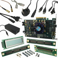
DK-DEV-4SGX230N Altera, DK-DEV-4SGX230N Datasheet - Page 566

DK-DEV-4SGX230N
Manufacturer Part Number
DK-DEV-4SGX230N
Description
KIT DEVELOPMENT STRATIX IV
Manufacturer
Altera
Series
Stratix® IVr
Type
FPGAr
Datasheets
1.EP4SGX110DF29C3N.pdf
(80 pages)
2.EP4SGX110DF29C3N.pdf
(1154 pages)
3.DK-DEV-4SGX230N.pdf
(2 pages)
4.DK-DEV-4SGX530N.pdf
(57 pages)
Specifications of DK-DEV-4SGX230N
Contents
Development Board, Universal Power Supply, Cables and Software
Silicon Manufacturer
Altera
Core Architecture
FPGA
Core Sub-architecture
Stratix
Silicon Core Number
EP4S
Silicon Family Name
Stratix IV GX
Rohs Compliant
Yes
For Use With/related Products
EP4SGX230K
Lead Free Status / RoHS Status
Lead free / RoHS Compliant
Other names
544-2594
Available stocks
Company
Part Number
Manufacturer
Quantity
Price
Company:
Part Number:
DK-DEV-4SGX230N
Manufacturer:
Altera
Quantity:
135
- EP4SGX110DF29C3N PDF datasheet
- EP4SGX110DF29C3N PDF datasheet #2
- DK-DEV-4SGX230N PDF datasheet #3
- DK-DEV-4SGX530N PDF datasheet #4
- Current page: 566 of 1154
- Download datasheet (32Mb)
1–122
Figure 1–102. Transceiver Datapath When in Deterministic Latency Mode
Stratix IV Device Handbook Volume 2: Transceivers
FPGA
Fabric
Deterministic Latency Mode
Stratix IV GX and GT devices have a deterministic latency option available for use in
high-speed serial interfaces such as CPRI (Common Public Radio Interface) and Open
Base Station Architecture Initiative Reference Point3 (OBSAI RP3). Both CPRI and
OBSAI RP3 protocols place stringent requirements on the amount of latency variation
that is permissible through a link implementing these protocols.
Figure 1–102
To implement this mode, select the Deterministic Latency option under the Which
Protocol will you be using? section in the ALTGX MegaWizard Plug-In Manager.
When you select this option, the transmitter channel is automatically placed in bit-slip
mode and Enable TX Phase Comp FIFO in register mode is automatically selected as
well. The receiver ’s phase compensation FIFO is automatically placed in the register
mode. In addition, an output port (rx_bitslipboundaryselectout[4:0]) from the
receiver’s word aligner and an input port (tx_bitslipboundaryselect[4:0]) for the
transmitter bit-slip circuitry are instantiated. The option for placing the transmitter
phase compensation FIFO in register mode is also available.
Transmitter Bit Slipping
The transmitter is bit slipped to achieve deterministic latency. Use the
tx_bitslipboundaryselect[4:0] port to set the number of bits that the transmitter
block needs to slip.
under different channel widths.
Table 1–44. Number of Transmitter Bits Allowed to be Slipped in Deterministic Latency Mode
Compensation
wrclk
TX Phase
shows the transceiver datapath when using deterministic latency mode.
FIFO
Channel Width
rdclk
16/20 bit
8/10 bit
Table 1–44
Byte Serializer
wrclk
Receiver Channel PCS
Transmitter Channel PCS
lists the number of bits that are allowed to be slipped
rdclk
Transmitter Channel Datapath
Receiver Channel Datapath
Chapter 1: Transceiver Architecture in Stratix IV Devices
8B/10B Encoder
Slip Zero
February 2011 Altera Corporation
19 bits
9 bits
Transceiver Block Architecture
Transmitter Channel
Receiver Channel
PMA
PMA
Related parts for DK-DEV-4SGX230N
Image
Part Number
Description
Manufacturer
Datasheet
Request
R

Part Number:
Description:
KIT DEV ARRIA II GX FPGA 2AGX125
Manufacturer:
Altera
Datasheet:

Part Number:
Description:
KIT DEV CYCLONE III LS EP3CLS200
Manufacturer:
Altera
Datasheet:

Part Number:
Description:
KIT DEV STRATIX IV FPGA 4SE530
Manufacturer:
Altera
Datasheet:

Part Number:
Description:
KIT DEV FPGA 2AGX260 W/6.375G TX
Manufacturer:
Altera
Datasheet:

Part Number:
Description:
KIT DEV MAX V 5M570Z
Manufacturer:
Altera
Datasheet:

Part Number:
Description:
KIT DEV STRATIX V FPGA 5SGXEA7
Manufacturer:
Altera
Datasheet:

Part Number:
Description:
KIT DEVELOPMENT STRATIX III
Manufacturer:
Altera
Datasheet:

Part Number:
Description:
KIT DEV ARRIA GX 1AGX60N
Manufacturer:
Altera
Datasheet:

Part Number:
Description:
KIT STARTER CYCLONE IV GX
Manufacturer:
Altera
Datasheet:

Part Number:
Description:
KIT DEVELOPMENT STRATIX IV
Manufacturer:
Altera
Datasheet:

Part Number:
Description:
CPLD, EP610 Family, ECMOS Process, 300 Gates, 16 Macro Cells, 16 Reg., 16 User I/Os, 5V Supply, 35 Speed Grade, 24DIP
Manufacturer:
Altera Corporation
Datasheet:

Part Number:
Description:
CPLD, EP610 Family, ECMOS Process, 300 Gates, 16 Macro Cells, 16 Reg., 16 User I/Os, 5V Supply, 15 Speed Grade, 24DIP
Manufacturer:
Altera Corporation
Datasheet:


