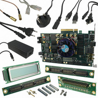
DK-DEV-4SGX230N Altera, DK-DEV-4SGX230N Datasheet - Page 194

DK-DEV-4SGX230N
Manufacturer Part Number
DK-DEV-4SGX230N
Description
KIT DEVELOPMENT STRATIX IV
Manufacturer
Altera
Series
Stratix® IVr
Type
FPGAr
Datasheets
1.EP4SGX110DF29C3N.pdf
(80 pages)
2.EP4SGX110DF29C3N.pdf
(1154 pages)
3.DK-DEV-4SGX230N.pdf
(2 pages)
4.DK-DEV-4SGX530N.pdf
(57 pages)
Specifications of DK-DEV-4SGX230N
Contents
Development Board, Universal Power Supply, Cables and Software
Silicon Manufacturer
Altera
Core Architecture
FPGA
Core Sub-architecture
Stratix
Silicon Core Number
EP4S
Silicon Family Name
Stratix IV GX
Rohs Compliant
Yes
For Use With/related Products
EP4SGX230K
Lead Free Status / RoHS Status
Lead free / RoHS Compliant
Other names
544-2594
Available stocks
Company
Part Number
Manufacturer
Quantity
Price
Company:
Part Number:
DK-DEV-4SGX230N
Manufacturer:
Altera
Quantity:
135
- EP4SGX110DF29C3N PDF datasheet
- EP4SGX110DF29C3N PDF datasheet #2
- DK-DEV-4SGX230N PDF datasheet #3
- DK-DEV-4SGX530N PDF datasheet #4
- Current page: 194 of 1154
- Download datasheet (32Mb)
6–22
Stratix IV Device Handbook Volume 1
Programmable I/O Delay
Open-Drain Output
Bus Hold
f
f
The following sections describe programmable IOE delay and programmable output
buffer delay.
Programmable IOE Delay
The Stratix IV device IOE includes programmable delays, shown in
page
increase clock-to-output times. Each pin can have a different input delay from
pin-to-input register or a delay from output register-to-output pin values to ensure
that the bus has the same delay going into or out of the device. This feature helps read
and time margins because it minimizes the uncertainties between signals in the bus.
For more information about programmable IOE delay specifications, refer to the
and Switching Characteristics for Stratix IV Devices
Programmable Output Buffer Delay
Stratix IV devices support delay chains built inside the single-ended output buffer, as
shown in
rising and falling edge delays of the output buffer, providing the ability to adjust the
output-buffer duty cycle, compensate channel-to-channel skew, reduce simultaneous
switching output (SSO) noise by deliberately introducing channel-to-channel skew,
and improve high-speed memory-interface timing margins. Stratix IV devices
support four levels of output buffer delay settings. The default setting is No Delay.
For more information about programmable output buffer delay specifications, refer to
the
Stratix IV devices provide an optional open-drain output (equivalent to an open
collector output) for each I/O pin. When configured as open drain, the logic value of
the output is either high-Z or 0. Typically, an external pull-up resistor is required to
provide logic high.
Each Stratix IV device I/O pin provides an optional bus-hold feature. Bus-hold
circuitry can weakly hold the signal on an I/O pin at its last-driven state. Because the
bus-hold feature holds the last-driven state of the pin until the next input signal is
present, you do not need an external pull-up or pull-down resistor to hold a signal
level when the bus is tri-stated.
Bus-hold circuitry also pulls non-driven pins away from the input threshold voltage
where noise can cause unintended high-frequency switching. You can select this
feature individually for each I/O pin. The bus-hold output drives no higher than
V
use the programmable pull-up option. Disable the bus-hold feature if the I/O pin is
configured for differential signals.
Bus-hold circuitry uses a resistor with a nominal resistance (R
7 k Ω to weakly pull the signal level to the last-driven state.
CCIO
DC and Switching Characteristics for Stratix IV Devices
6–18, that you can activate to ensure zero hold times, minimize setup times, or
to prevent over-driving signals. If you enable the bus-hold feature, you cannot
Figure 6–17 on page
6–18. The delay chains can independently control the
chapter.
Chapter 6: I/O Features in Stratix IV Devices
chapter.
February 2011 Altera Corporation
BH
) of approximately
Figure 6–17 on
I/O Structure
DC
Related parts for DK-DEV-4SGX230N
Image
Part Number
Description
Manufacturer
Datasheet
Request
R

Part Number:
Description:
KIT DEV ARRIA II GX FPGA 2AGX125
Manufacturer:
Altera
Datasheet:

Part Number:
Description:
KIT DEV CYCLONE III LS EP3CLS200
Manufacturer:
Altera
Datasheet:

Part Number:
Description:
KIT DEV STRATIX IV FPGA 4SE530
Manufacturer:
Altera
Datasheet:

Part Number:
Description:
KIT DEV FPGA 2AGX260 W/6.375G TX
Manufacturer:
Altera
Datasheet:

Part Number:
Description:
KIT DEV MAX V 5M570Z
Manufacturer:
Altera
Datasheet:

Part Number:
Description:
KIT DEV STRATIX V FPGA 5SGXEA7
Manufacturer:
Altera
Datasheet:

Part Number:
Description:
KIT DEVELOPMENT STRATIX III
Manufacturer:
Altera
Datasheet:

Part Number:
Description:
KIT DEV ARRIA GX 1AGX60N
Manufacturer:
Altera
Datasheet:

Part Number:
Description:
KIT STARTER CYCLONE IV GX
Manufacturer:
Altera
Datasheet:

Part Number:
Description:
KIT DEVELOPMENT STRATIX IV
Manufacturer:
Altera
Datasheet:

Part Number:
Description:
CPLD, EP610 Family, ECMOS Process, 300 Gates, 16 Macro Cells, 16 Reg., 16 User I/Os, 5V Supply, 35 Speed Grade, 24DIP
Manufacturer:
Altera Corporation
Datasheet:

Part Number:
Description:
CPLD, EP610 Family, ECMOS Process, 300 Gates, 16 Macro Cells, 16 Reg., 16 User I/Os, 5V Supply, 15 Speed Grade, 24DIP
Manufacturer:
Altera Corporation
Datasheet:


