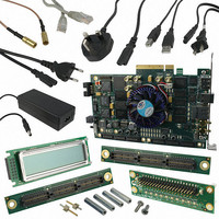
DK-DEV-4SGX230N Altera, DK-DEV-4SGX230N Datasheet - Page 542

DK-DEV-4SGX230N
Manufacturer Part Number
DK-DEV-4SGX230N
Description
KIT DEVELOPMENT STRATIX IV
Manufacturer
Altera
Series
Stratix® IVr
Type
FPGAr
Datasheets
1.EP4SGX110DF29C3N.pdf
(80 pages)
2.EP4SGX110DF29C3N.pdf
(1154 pages)
3.DK-DEV-4SGX230N.pdf
(2 pages)
4.DK-DEV-4SGX530N.pdf
(57 pages)
Specifications of DK-DEV-4SGX230N
Contents
Development Board, Universal Power Supply, Cables and Software
Silicon Manufacturer
Altera
Core Architecture
FPGA
Core Sub-architecture
Stratix
Silicon Core Number
EP4S
Silicon Family Name
Stratix IV GX
Rohs Compliant
Yes
For Use With/related Products
EP4SGX230K
Lead Free Status / RoHS Status
Lead free / RoHS Compliant
Other names
544-2594
Available stocks
Company
Part Number
Manufacturer
Quantity
Price
Company:
Part Number:
DK-DEV-4SGX230N
Manufacturer:
Altera
Quantity:
135
- EP4SGX110DF29C3N PDF datasheet
- EP4SGX110DF29C3N PDF datasheet #2
- DK-DEV-4SGX230N PDF datasheet #3
- DK-DEV-4SGX530N PDF datasheet #4
- Current page: 542 of 1154
- Download datasheet (32Mb)
1–98
Figure 1–86. User-Controlled Byte Ordering in Basic Double-Width Mode
Stratix IV Device Handbook Volume 2: Transceivers
tx_datain[31:16]
tx_datain[15:0]
(MSByte)
(LSByte)
D2D3
D0D1
B1B2
D4D5
D8D9
D6D7
Unlike word-alignment-based byte ordering, user-controlled byte ordering provides
control to the user logic to restore correct byte ordering at the receiver. When enabled,
an rx_enabyteord port is available that you can use to trigger the byte ordering
operation. A rising edge on the rx_enabyteord port triggers the byte ordering block.
After a rising edge on the rx_enabyteord signal, if the byte ordering block finds the
first data byte that matches the programmed byte ordering pattern in the MSByte
position of the byte-deserialized data, it inserts one programmed PAD pattern to push
the byte ordering pattern in the LSByte position. If the byte ordering block finds the
first data byte that matches the programmed byte ordering pattern in the LSByte
position of the byte-deserialized data, it considers the data to be byte ordered and
does not insert any PAD byte. In either case, the byte ordering block asserts the
rx_byteorderalignstatus signal.
Figure 1–86
Receiver Phase Compensation FIFO
The receiver phase compensation FIFO in each channel ensures reliable transfer of
data and status signals between the receiver channel and the FPGA fabric. The
receiver phase compensation FIFO compensates for the phase difference between the
parallel receiver PCS clock (FIFO write clock) and the FPGA fabric clock (FIFO read
clock).
The receiver phase compensation FIFO operates in one of the following two modes:
■
■
B1B2
Low latency mode—The Quartus II software automatically configures the receiver
phase compensation FIFO in low latency mode in all functional modes. In this
mode, the FIFO is four words deep and the latency through the FIFO is two to
three parallel clock cycles (pending characterization).
High latency mode—In this mode, the FIFO is eight words deep and the latency
through the FIFO is four to five parallel clock cycles (pending characterization).
xxxx
Transmitter
User-Controlled Byte Ordering
Serializer
Byte
shows user-controlled byte ordering in Basic double-width Mode.
Channel
Deserializer
Byte
Receiver
D0D1
xxxx
B1B2
D2D3
D4D5
D6D7
rx_byteorderalignstatus
B1B2
D8D9
Chapter 1: Transceiver Architecture in Stratix IV Devices
rx_enabyteord
Ordering
Byte
D0D1
xxxx
D2D3
P1P2
February 2011 Altera Corporation
D4D5
B1B2
Transceiver Block Architecture
D8D9
D6D7
B1B2
xxxx
rx_dataout [31:16]
rx_dataout[15:0]
(MSByte)
(LSByte)
Related parts for DK-DEV-4SGX230N
Image
Part Number
Description
Manufacturer
Datasheet
Request
R

Part Number:
Description:
KIT DEV ARRIA II GX FPGA 2AGX125
Manufacturer:
Altera
Datasheet:

Part Number:
Description:
KIT DEV CYCLONE III LS EP3CLS200
Manufacturer:
Altera
Datasheet:

Part Number:
Description:
KIT DEV STRATIX IV FPGA 4SE530
Manufacturer:
Altera
Datasheet:

Part Number:
Description:
KIT DEV FPGA 2AGX260 W/6.375G TX
Manufacturer:
Altera
Datasheet:

Part Number:
Description:
KIT DEV MAX V 5M570Z
Manufacturer:
Altera
Datasheet:

Part Number:
Description:
KIT DEV STRATIX V FPGA 5SGXEA7
Manufacturer:
Altera
Datasheet:

Part Number:
Description:
KIT DEVELOPMENT STRATIX III
Manufacturer:
Altera
Datasheet:

Part Number:
Description:
KIT DEV ARRIA GX 1AGX60N
Manufacturer:
Altera
Datasheet:

Part Number:
Description:
KIT STARTER CYCLONE IV GX
Manufacturer:
Altera
Datasheet:

Part Number:
Description:
KIT DEVELOPMENT STRATIX IV
Manufacturer:
Altera
Datasheet:

Part Number:
Description:
CPLD, EP610 Family, ECMOS Process, 300 Gates, 16 Macro Cells, 16 Reg., 16 User I/Os, 5V Supply, 35 Speed Grade, 24DIP
Manufacturer:
Altera Corporation
Datasheet:

Part Number:
Description:
CPLD, EP610 Family, ECMOS Process, 300 Gates, 16 Macro Cells, 16 Reg., 16 User I/Os, 5V Supply, 15 Speed Grade, 24DIP
Manufacturer:
Altera Corporation
Datasheet:


