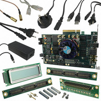
DK-DEV-4SGX230N Altera, DK-DEV-4SGX230N Datasheet - Page 262

DK-DEV-4SGX230N
Manufacturer Part Number
DK-DEV-4SGX230N
Description
KIT DEVELOPMENT STRATIX IV
Manufacturer
Altera
Series
Stratix® IVr
Type
FPGAr
Datasheets
1.EP4SGX110DF29C3N.pdf
(80 pages)
2.EP4SGX110DF29C3N.pdf
(1154 pages)
3.DK-DEV-4SGX230N.pdf
(2 pages)
4.DK-DEV-4SGX530N.pdf
(57 pages)
Specifications of DK-DEV-4SGX230N
Contents
Development Board, Universal Power Supply, Cables and Software
Silicon Manufacturer
Altera
Core Architecture
FPGA
Core Sub-architecture
Stratix
Silicon Core Number
EP4S
Silicon Family Name
Stratix IV GX
Rohs Compliant
Yes
For Use With/related Products
EP4SGX230K
Lead Free Status / RoHS Status
Lead free / RoHS Compliant
Other names
544-2594
Available stocks
Company
Part Number
Manufacturer
Quantity
Price
Company:
Part Number:
DK-DEV-4SGX230N
Manufacturer:
Altera
Quantity:
135
- EP4SGX110DF29C3N PDF datasheet
- EP4SGX110DF29C3N PDF datasheet #2
- DK-DEV-4SGX230N PDF datasheet #3
- DK-DEV-4SGX530N PDF datasheet #4
- Current page: 262 of 1154
- Download datasheet (32Mb)
7–42
Stratix IV Device Handbook Volume 1
Phase Offset Control
f
There are eight different frequency modes for the Stratix IV DLL, as listed in
Table
frequency mode 0, 1, 2, and 3, the 6-bit DQS delay settings vary with PVT to
implement the phase-shift delay. In frequency modes 4, 5, 6, and 7, only 5 bits of the
DQS delay settings vary with PVT to implement the phase-shift delay; the most
significant bit of the DQS delay setting is set to 0.
Table 7–18. Stratix IV DLL Frequency Modes
For the frequency range of each mode, refer to the
Stratix IV Devices
For 0° shift, the DQS/CQ signal bypasses both the DLL and DQS logic blocks. The
Quartus II software automatically sets the DQ input delay chains so that the skew
between the DQ and DQS/CQ pin at the DQ IOE registers is negligible when 0° shift
is implemented. You can feed the DQS delay settings to the DQS logic block and logic
array.
The shifted DQS/CQ signal goes to the DQS bus to clock the IOE input registers of the
DQ pins. The signal can also go into the logic array for resynchronization if you are
not using IOE resynchronization registers. The shifted CQn signal can only go to the
negative-edge input register in the DQ IOE and is only used for QDR II+ and QDR II
SRAM interfaces.
Each DLL has two phase-offset modules and can provide two separate DQS delay
settings with independent offsets, one for the top and bottom I/O bank and one for
the left and right I/O bank, so you can fine-tune the DQS phase-shift settings between
two different sides of the device. Even though you have independent phase offset
control, the frequency of the interface using the same DLL must be the same. Use the
phase offset control module for making small shifts to the input signal and use the
DQS phase-shift circuitry for larger signal shifts. For example, if the DLL only offers a
multiple of 30° phase shift, but your interface needs a 67.5° phase shift on the DQS
signal, you can use two delay chains in the DQS logic blocks to give you 60° phase
shift and use the phase offset control feature to implement the extra 7.5° phase shift.
7–18. Each frequency mode provides different phase shift selections. In
Frequency Mode
0
1
2
3
4
5
6
7
chapter.
Available Phase Shift
22.5, 45, 67.5, 90
60, 120, 180, 240
36, 72, 108, 144
45, 90, 135, 180
36, 72, 108, 144
45, 90, 135, 180
30, 60, 90, 120
30, 60, 90, 120
Chapter 7: External Memory Interfaces in Stratix IV Devices
DC and Switching Characteristics for
Stratix IV External Memory Interface Features
February 2011 Altera Corporation
Number of Delay Chains
16
12
10
12
10
8
8
6
Related parts for DK-DEV-4SGX230N
Image
Part Number
Description
Manufacturer
Datasheet
Request
R

Part Number:
Description:
KIT DEV ARRIA II GX FPGA 2AGX125
Manufacturer:
Altera
Datasheet:

Part Number:
Description:
KIT DEV CYCLONE III LS EP3CLS200
Manufacturer:
Altera
Datasheet:

Part Number:
Description:
KIT DEV STRATIX IV FPGA 4SE530
Manufacturer:
Altera
Datasheet:

Part Number:
Description:
KIT DEV FPGA 2AGX260 W/6.375G TX
Manufacturer:
Altera
Datasheet:

Part Number:
Description:
KIT DEV MAX V 5M570Z
Manufacturer:
Altera
Datasheet:

Part Number:
Description:
KIT DEV STRATIX V FPGA 5SGXEA7
Manufacturer:
Altera
Datasheet:

Part Number:
Description:
KIT DEVELOPMENT STRATIX III
Manufacturer:
Altera
Datasheet:

Part Number:
Description:
KIT DEV ARRIA GX 1AGX60N
Manufacturer:
Altera
Datasheet:

Part Number:
Description:
KIT STARTER CYCLONE IV GX
Manufacturer:
Altera
Datasheet:

Part Number:
Description:
KIT DEVELOPMENT STRATIX IV
Manufacturer:
Altera
Datasheet:

Part Number:
Description:
CPLD, EP610 Family, ECMOS Process, 300 Gates, 16 Macro Cells, 16 Reg., 16 User I/Os, 5V Supply, 35 Speed Grade, 24DIP
Manufacturer:
Altera Corporation
Datasheet:

Part Number:
Description:
CPLD, EP610 Family, ECMOS Process, 300 Gates, 16 Macro Cells, 16 Reg., 16 User I/Os, 5V Supply, 15 Speed Grade, 24DIP
Manufacturer:
Altera Corporation
Datasheet:


