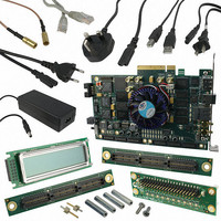
DK-DEV-4SGX230N Altera, DK-DEV-4SGX230N Datasheet - Page 482

DK-DEV-4SGX230N
Manufacturer Part Number
DK-DEV-4SGX230N
Description
KIT DEVELOPMENT STRATIX IV
Manufacturer
Altera
Series
Stratix® IVr
Type
FPGAr
Datasheets
1.EP4SGX110DF29C3N.pdf
(80 pages)
2.EP4SGX110DF29C3N.pdf
(1154 pages)
3.DK-DEV-4SGX230N.pdf
(2 pages)
4.DK-DEV-4SGX530N.pdf
(57 pages)
Specifications of DK-DEV-4SGX230N
Contents
Development Board, Universal Power Supply, Cables and Software
Silicon Manufacturer
Altera
Core Architecture
FPGA
Core Sub-architecture
Stratix
Silicon Core Number
EP4S
Silicon Family Name
Stratix IV GX
Rohs Compliant
Yes
For Use With/related Products
EP4SGX230K
Lead Free Status / RoHS Status
Lead free / RoHS Compliant
Other names
544-2594
Available stocks
Company
Part Number
Manufacturer
Quantity
Price
Company:
Part Number:
DK-DEV-4SGX230N
Manufacturer:
Altera
Quantity:
135
- EP4SGX110DF29C3N PDF datasheet
- EP4SGX110DF29C3N PDF datasheet #2
- DK-DEV-4SGX230N PDF datasheet #3
- DK-DEV-4SGX530N PDF datasheet #4
- Current page: 482 of 1154
- Download datasheet (32Mb)
1–38
Stratix IV Device Handbook Volume 2: Transceivers
f
Figure 1–34. DC-Coupled Link
The Stratix IV GX and GT transmitter can be DC-coupled to a Stratix IV GX and GT
receiver for the entire operating data rate range of Stratix IV GX, from 600 Mbps to
8.5 Gbps.
The Stratix IV GT transmitter can be DC-coupled to the Stratix IV GT receiver for the
entire data rate range of 600 Mbps to 11.3 Gbps with Tx Vcm = 0.65 V and
Rx Vcm = 0.82 V.
For more information on the DC coupling capabilities of the Stratix IV GT device,
refer to
The Stratix IV GX and GT transmitter buffers have a built-in receiver detection circuit
for use in the PCIe mode for Gen1 and Gen2 data rates. This circuit detects if there is a
receiver downstream by sending out a pulse on the common mode of the transmitter
and monitoring the reflection. This mode requires the transmitter buffer to be
tri-stated (in Electrical Idle mode), OCT utilization, and a 125 MHz fixedclk signal.
You can enable this feature in PCIe mode by setting the tx_forceelecidle and
tx_detectrxloopback ports to 1'b1. Receiver detect circuitry is active only in the P1
power state.
For more information about power states, refer to the PCIe 2.0 specification.
In the P1 power state, the transmitter output buffer is tri-stated because the
transmitter output buffer is in electrical idle. A high on the tx_detectrxloopback port
triggers the receiver detect circuitry to alter the transmitter output buffer V
sudden change in V
transmitter buffer output. If a receiver (that complies with PCIe input impedance
requirements) is present at the far end, the time constant of the step voltage is higher.
If a receiver is not present or is powered down, the time constant of the step voltage is
lower. The receiver detect circuitry snoops the transmitter buffer output for the time
constant of the step voltage to detect the presence of the receiver at the far end. A high
PCIe Receiver Detect
Table 1–23 on page
Transmitter
TX Termination
CM
effectively appears as a step voltage at the tri-stated
TX
V
CM
1–48.
Physical Medium
Physical Medium
Chapter 1: Transceiver Architecture in Stratix IV Devices
RX
V
CM
February 2011 Altera Corporation
RX Termination
Transceiver Block Architecture
Receiver
CM
. The
Related parts for DK-DEV-4SGX230N
Image
Part Number
Description
Manufacturer
Datasheet
Request
R

Part Number:
Description:
KIT DEV ARRIA II GX FPGA 2AGX125
Manufacturer:
Altera
Datasheet:

Part Number:
Description:
KIT DEV CYCLONE III LS EP3CLS200
Manufacturer:
Altera
Datasheet:

Part Number:
Description:
KIT DEV STRATIX IV FPGA 4SE530
Manufacturer:
Altera
Datasheet:

Part Number:
Description:
KIT DEV FPGA 2AGX260 W/6.375G TX
Manufacturer:
Altera
Datasheet:

Part Number:
Description:
KIT DEV MAX V 5M570Z
Manufacturer:
Altera
Datasheet:

Part Number:
Description:
KIT DEV STRATIX V FPGA 5SGXEA7
Manufacturer:
Altera
Datasheet:

Part Number:
Description:
KIT DEVELOPMENT STRATIX III
Manufacturer:
Altera
Datasheet:

Part Number:
Description:
KIT DEV ARRIA GX 1AGX60N
Manufacturer:
Altera
Datasheet:

Part Number:
Description:
KIT STARTER CYCLONE IV GX
Manufacturer:
Altera
Datasheet:

Part Number:
Description:
KIT DEVELOPMENT STRATIX IV
Manufacturer:
Altera
Datasheet:

Part Number:
Description:
CPLD, EP610 Family, ECMOS Process, 300 Gates, 16 Macro Cells, 16 Reg., 16 User I/Os, 5V Supply, 35 Speed Grade, 24DIP
Manufacturer:
Altera Corporation
Datasheet:

Part Number:
Description:
CPLD, EP610 Family, ECMOS Process, 300 Gates, 16 Macro Cells, 16 Reg., 16 User I/Os, 5V Supply, 15 Speed Grade, 24DIP
Manufacturer:
Altera Corporation
Datasheet:


