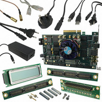
DK-DEV-4SGX230N Altera, DK-DEV-4SGX230N Datasheet - Page 596

DK-DEV-4SGX230N
Manufacturer Part Number
DK-DEV-4SGX230N
Description
KIT DEVELOPMENT STRATIX IV
Manufacturer
Altera
Series
Stratix® IVr
Type
FPGAr
Datasheets
1.EP4SGX110DF29C3N.pdf
(80 pages)
2.EP4SGX110DF29C3N.pdf
(1154 pages)
3.DK-DEV-4SGX230N.pdf
(2 pages)
4.DK-DEV-4SGX530N.pdf
(57 pages)
Specifications of DK-DEV-4SGX230N
Contents
Development Board, Universal Power Supply, Cables and Software
Silicon Manufacturer
Altera
Core Architecture
FPGA
Core Sub-architecture
Stratix
Silicon Core Number
EP4S
Silicon Family Name
Stratix IV GX
Rohs Compliant
Yes
For Use With/related Products
EP4SGX230K
Lead Free Status / RoHS Status
Lead free / RoHS Compliant
Other names
544-2594
Available stocks
Company
Part Number
Manufacturer
Quantity
Price
Company:
Part Number:
DK-DEV-4SGX230N
Manufacturer:
Altera
Quantity:
135
- EP4SGX110DF29C3N PDF datasheet
- EP4SGX110DF29C3N PDF datasheet #2
- DK-DEV-4SGX230N PDF datasheet #3
- DK-DEV-4SGX530N PDF datasheet #4
- Current page: 596 of 1154
- Download datasheet (32Mb)
1–152
Stratix IV Device Handbook Volume 2: Transceivers
f
f
1
Table 1–57
configured using the Fast Passive Parallel (FPP) configuration scheme at 125 MHz.
Table 1–57. Typical Configuration Times for Stratix IV GX Devices Configured with Fast Passive
Parallel
For more information about the FPP configuration scheme, refer to the
Design Security, Remote System Upgrades in Stratix IV Devices
Most flash memories available can run up to 100 MHz. To configure the
Stratix IV GX and GT device at 125 MHz, Altera recommends using a MAX II device
to convert the 16-bit flash memory output at 62.5 MHz to 8-bit configuration data
input to the Stratix IV GX and GT device at 125 MHz.
The PCI Express Electrical Gold Test requires the v2.0 CBB to be connected to the
Device Under Test (DUT). The CBB sends out a 100 MHz signal for 1 ms to indicate
the Link Training and Status State Machine (LTSSM) of the downstream device Under
Test (DUT) to transition to several polling compliance states. Under these states, the
DUT sends out data at Gen1, Gen2 (with -3.5db de-emphasis), and Gen2 (with -6 db
de-emphasis) rates, which can be observed in the scope to confirm electrical signal
compliance. The CBB is DC-coupled to the downstream receiver.
When you use the Stratix IV GX and GT device as DUT, because of being DC-coupled
to CBB with a different common mode level, the Stratix IV GX and GT receiver does
not receive the required V
that implements LTSSM cannot transition to the multiple polling compliance states to
complete the test. Therefore, when testing with the CBB, force the LTSSM
implemented in the FPGA fabric to transfer to different polling compliance states
using an external push button or user logic.
If you use the Stratix IV GX and GT PCIe hard IP block, assert the test_in[6] port of
the PCIe Compiler-generated wrapper file in your design. Asserting this port forces
the LTSSM within the hard IP block to transition to these states. The test_in[6] port
must be asserted for a minimum of 16 ns and less than 24 ms.
For more information about the PCIe hard IP block, refer to the
User
PCI Express Electrical Gold Test with Compliance Base Board (CBB)
Guide.
Stratix IV GX
EP4SGX110
EP4SGX230
EP4SGX290
EP4SGX360
EP4SGX530
EP4SGX70
lists the typical configuration times for Stratix IV GX devices when
CM
(0.85 V) to detect the signal. The logic in the FPGA fabric
EP4S(40/100)G2
EP4S(40/100)G5
Stratix IV GT
EP4S100G3
EP4S100G4
Chapter 1: Transceiver Architecture in Stratix IV Devices
—
—
chapter.
February 2011 Altera Corporation
Configuration Time (ms)
PCI Express Compiler
Transceiver Block Architecture
128
128
172
48
48
95
Configuration,
Related parts for DK-DEV-4SGX230N
Image
Part Number
Description
Manufacturer
Datasheet
Request
R

Part Number:
Description:
KIT DEV ARRIA II GX FPGA 2AGX125
Manufacturer:
Altera
Datasheet:

Part Number:
Description:
KIT DEV CYCLONE III LS EP3CLS200
Manufacturer:
Altera
Datasheet:

Part Number:
Description:
KIT DEV STRATIX IV FPGA 4SE530
Manufacturer:
Altera
Datasheet:

Part Number:
Description:
KIT DEV FPGA 2AGX260 W/6.375G TX
Manufacturer:
Altera
Datasheet:

Part Number:
Description:
KIT DEV MAX V 5M570Z
Manufacturer:
Altera
Datasheet:

Part Number:
Description:
KIT DEV STRATIX V FPGA 5SGXEA7
Manufacturer:
Altera
Datasheet:

Part Number:
Description:
KIT DEVELOPMENT STRATIX III
Manufacturer:
Altera
Datasheet:

Part Number:
Description:
KIT DEV ARRIA GX 1AGX60N
Manufacturer:
Altera
Datasheet:

Part Number:
Description:
KIT STARTER CYCLONE IV GX
Manufacturer:
Altera
Datasheet:

Part Number:
Description:
KIT DEVELOPMENT STRATIX IV
Manufacturer:
Altera
Datasheet:

Part Number:
Description:
CPLD, EP610 Family, ECMOS Process, 300 Gates, 16 Macro Cells, 16 Reg., 16 User I/Os, 5V Supply, 35 Speed Grade, 24DIP
Manufacturer:
Altera Corporation
Datasheet:

Part Number:
Description:
CPLD, EP610 Family, ECMOS Process, 300 Gates, 16 Macro Cells, 16 Reg., 16 User I/Os, 5V Supply, 15 Speed Grade, 24DIP
Manufacturer:
Altera Corporation
Datasheet:


