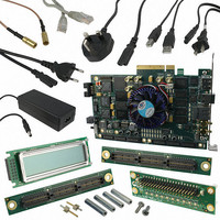
DK-DEV-4SGX230N Altera, DK-DEV-4SGX230N Datasheet - Page 584

DK-DEV-4SGX230N
Manufacturer Part Number
DK-DEV-4SGX230N
Description
KIT DEVELOPMENT STRATIX IV
Manufacturer
Altera
Series
Stratix® IVr
Type
FPGAr
Datasheets
1.EP4SGX110DF29C3N.pdf
(80 pages)
2.EP4SGX110DF29C3N.pdf
(1154 pages)
3.DK-DEV-4SGX230N.pdf
(2 pages)
4.DK-DEV-4SGX530N.pdf
(57 pages)
Specifications of DK-DEV-4SGX230N
Contents
Development Board, Universal Power Supply, Cables and Software
Silicon Manufacturer
Altera
Core Architecture
FPGA
Core Sub-architecture
Stratix
Silicon Core Number
EP4S
Silicon Family Name
Stratix IV GX
Rohs Compliant
Yes
For Use With/related Products
EP4SGX230K
Lead Free Status / RoHS Status
Lead free / RoHS Compliant
Other names
544-2594
Available stocks
Company
Part Number
Manufacturer
Quantity
Price
Company:
Part Number:
DK-DEV-4SGX230N
Manufacturer:
Altera
Quantity:
135
- EP4SGX110DF29C3N PDF datasheet
- EP4SGX110DF29C3N PDF datasheet #2
- DK-DEV-4SGX230N PDF datasheet #3
- DK-DEV-4SGX530N PDF datasheet #4
- Current page: 584 of 1154
- Download datasheet (32Mb)
1–140
Stratix IV Device Handbook Volume 2: Transceivers
1
1
If you do not select the Enable electrical idle inference functionality option in the
ALTGX MegaWizard Plug-In Manager, the Electrical Idle Inference module is
disabled. In this case, the rx_signaldetect signal from the signal detect circuitry in
the receiver buffer is inverted and driven as the pipeelecidle signal.
Recommendation When Using the Electrical Idle Inference Block
In a PCIe link, when operating at Gen2 data rate, the downstream device can go into
the Disable state after instruction from the upper layer. Once in the Disable state, the
downstream device must detect an Electrical Idle Exit condition to go into the Detect
state. At this same time, the upstream device can be directed by the upper layer to go
into the Detect state and start transmitting the COM symbols to the downstream
device at Gen 1 data rate.
The Disable and Detect states are different states of the Link Training and Status State
Machine as described by the PCIe Base Specification Rev 2.0.
The COM symbol is an 8B/10B encoded value of K28.5 and is part of the training
sequences TS1 and TS2 as described by the PCIe Base Specification Rev 2.0.
When the Stratix IV GX and GT device is operating as a downstream device at PCIe
Gen 2 data rates and if it goes into the Disable State, the Stratix IV GX and GT receiver
must receive an Electrical Idle Exit condition in order to move out of the Disable state.
For the Stratix IV GX and GT receiver, the Electrical Idle Exit condition is achieved
when COM symbols are received from the upstream device. However, after the
Disable state is achieved by the Stratix IV GX and GT receiver (the downstream
device) during Gen 2 data rate operation, and if at the same time the upstream device
is directed to transition to the Detect state, the upstream device starts to send COM
symbols at Gen 1 data rate. Consequently, the Stratix IV GX and GT receiver (the
downstream device) does not recognize the COM symbols as it is operating at Gen 2
data rate. To avoid this scenario, the Link Training Status State Machine (LTSSM) in
the FPGA fabric of Stratix IV GX and GT receiver (the downstream device) must be
implemented in such a way that whenever the downstream device goes into the
Disable state and the upstream device is directed to go into the Detect state, the
rateswitch signal must be transitioned from high to low. This allows the
Stratix IV GX and GT receiver (the downstream device) to move from Gen 2 to Gen 1
data rate. Subsequently, the Stratix IV GX and GT receiver (the downstream device)
recognizes the COM symbols being sent by the upstream device at Gen 1 data rates
and moves from the Disable state to the Detect state.
The PCIe functional mode supports the following additional features when
configured for 5 Gbps data rate:
■
■
■
Dynamic switch between 2.5 Gbps and 5 Gbps signaling rate
Dynamically selectable transmitter margining for differential output voltage
control
Dynamically selectable transmitter buffer de-emphasis of -3.5 db and -6 dB
PCIe Gen2 (5 Gbps) Support
Chapter 1: Transceiver Architecture in Stratix IV Devices
February 2011 Altera Corporation
Transceiver Block Architecture
Related parts for DK-DEV-4SGX230N
Image
Part Number
Description
Manufacturer
Datasheet
Request
R

Part Number:
Description:
KIT DEV ARRIA II GX FPGA 2AGX125
Manufacturer:
Altera
Datasheet:

Part Number:
Description:
KIT DEV CYCLONE III LS EP3CLS200
Manufacturer:
Altera
Datasheet:

Part Number:
Description:
KIT DEV STRATIX IV FPGA 4SE530
Manufacturer:
Altera
Datasheet:

Part Number:
Description:
KIT DEV FPGA 2AGX260 W/6.375G TX
Manufacturer:
Altera
Datasheet:

Part Number:
Description:
KIT DEV MAX V 5M570Z
Manufacturer:
Altera
Datasheet:

Part Number:
Description:
KIT DEV STRATIX V FPGA 5SGXEA7
Manufacturer:
Altera
Datasheet:

Part Number:
Description:
KIT DEVELOPMENT STRATIX III
Manufacturer:
Altera
Datasheet:

Part Number:
Description:
KIT DEV ARRIA GX 1AGX60N
Manufacturer:
Altera
Datasheet:

Part Number:
Description:
KIT STARTER CYCLONE IV GX
Manufacturer:
Altera
Datasheet:

Part Number:
Description:
KIT DEVELOPMENT STRATIX IV
Manufacturer:
Altera
Datasheet:

Part Number:
Description:
CPLD, EP610 Family, ECMOS Process, 300 Gates, 16 Macro Cells, 16 Reg., 16 User I/Os, 5V Supply, 35 Speed Grade, 24DIP
Manufacturer:
Altera Corporation
Datasheet:

Part Number:
Description:
CPLD, EP610 Family, ECMOS Process, 300 Gates, 16 Macro Cells, 16 Reg., 16 User I/Os, 5V Supply, 15 Speed Grade, 24DIP
Manufacturer:
Altera Corporation
Datasheet:


