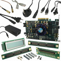
DK-DEV-4SGX230N Altera, DK-DEV-4SGX230N Datasheet - Page 316

DK-DEV-4SGX230N
Manufacturer Part Number
DK-DEV-4SGX230N
Description
KIT DEVELOPMENT STRATIX IV
Manufacturer
Altera
Series
Stratix® IVr
Type
FPGAr
Datasheets
1.EP4SGX110DF29C3N.pdf
(80 pages)
2.EP4SGX110DF29C3N.pdf
(1154 pages)
3.DK-DEV-4SGX230N.pdf
(2 pages)
4.DK-DEV-4SGX530N.pdf
(57 pages)
Specifications of DK-DEV-4SGX230N
Contents
Development Board, Universal Power Supply, Cables and Software
Silicon Manufacturer
Altera
Core Architecture
FPGA
Core Sub-architecture
Stratix
Silicon Core Number
EP4S
Silicon Family Name
Stratix IV GX
Rohs Compliant
Yes
For Use With/related Products
EP4SGX230K
Lead Free Status / RoHS Status
Lead free / RoHS Compliant
Other names
544-2594
Available stocks
Company
Part Number
Manufacturer
Quantity
Price
Company:
Part Number:
DK-DEV-4SGX230N
Manufacturer:
Altera
Quantity:
135
- EP4SGX110DF29C3N PDF datasheet
- EP4SGX110DF29C3N PDF datasheet #2
- DK-DEV-4SGX230N PDF datasheet #3
- DK-DEV-4SGX530N PDF datasheet #4
- Current page: 316 of 1154
- Download datasheet (32Mb)
8–38
Differential Pin Placement Guidelines
Stratix IV Device Handbook Volume 1
Guidelines for DPA-Enabled Differential Channels
1
To ensure proper high-speed operation, differential pin placement guidelines have
been established. The Quartus II compiler automatically checks that these guidelines
are followed and issues an error message if they are not met.
This section is divided into pin placement guidelines with and without DPA usage
because DPA usage adds some constraints on the placement of high-speed differential
channels.
DPA-enabled differential channels refer to DPA mode or soft-CDR mode; DPA
disabled channels refer to non-DPA mode.
The Stratix IV device family has differential receivers and transmitters in I/O banks
on the left and right sides of the device. Each receiver has a dedicated DPA circuit to
align the phase of the clock to the data phase of its associated channel. When you use
DPA-enabled channels in differential banks, you must adhere to the guidelines listed
in the following sections.
DPA-Enabled Channels and Single-Ended I/Os
When you enable a DPA channel in a bank, both single-ended I/Os and differential
I/O standards are allowed in the bank.
■
■
■
DPA-Enabled Channel Driving Distance
If the number of DPA channels driven by each left and right PLL exceeds 25 LAB
rows, Altera recommends implementing data realignment (bit slip) circuitry for all
the DPA channels.
Using Corner and Center Left and Right PLLs
If a differential bank is being driven by two left and right PLLs, where the corner left
and right PLL is driving one group and the center left and right PLL is driving
another group, there must be at least one row of separation between the two groups
of DPA-enabled channels (refer to
independent frequencies.
Single-ended I/Os are allowed in the same I/O bank, as long as the single-ended
I/O standard uses the same V
Single-ended inputs can be in the same logic array block (LAB) row as a
differential channel using the SERDES circuitry.
DDIO can be placed within the same LAB row as a SERDES differential channel
but half rate DDIO (single data rate) output pins cannot be placed within the same
LAB row as a receiver SERDES differential channel. The input register must be
implemented within the FPGA fabric logic.
Chapter 8: High-Speed Differential I/O Interfaces and DPA in Stratix IV Devices
CCIO
Figure
as the DPA-enabled differential I/O bank.
8–31). The two groups can operate at
Differential Pin Placement Guidelines
February 2011 Altera Corporation
Related parts for DK-DEV-4SGX230N
Image
Part Number
Description
Manufacturer
Datasheet
Request
R

Part Number:
Description:
KIT DEV ARRIA II GX FPGA 2AGX125
Manufacturer:
Altera
Datasheet:

Part Number:
Description:
KIT DEV CYCLONE III LS EP3CLS200
Manufacturer:
Altera
Datasheet:

Part Number:
Description:
KIT DEV STRATIX IV FPGA 4SE530
Manufacturer:
Altera
Datasheet:

Part Number:
Description:
KIT DEV FPGA 2AGX260 W/6.375G TX
Manufacturer:
Altera
Datasheet:

Part Number:
Description:
KIT DEV MAX V 5M570Z
Manufacturer:
Altera
Datasheet:

Part Number:
Description:
KIT DEV STRATIX V FPGA 5SGXEA7
Manufacturer:
Altera
Datasheet:

Part Number:
Description:
KIT DEVELOPMENT STRATIX III
Manufacturer:
Altera
Datasheet:

Part Number:
Description:
KIT DEV ARRIA GX 1AGX60N
Manufacturer:
Altera
Datasheet:

Part Number:
Description:
KIT STARTER CYCLONE IV GX
Manufacturer:
Altera
Datasheet:

Part Number:
Description:
KIT DEVELOPMENT STRATIX IV
Manufacturer:
Altera
Datasheet:

Part Number:
Description:
CPLD, EP610 Family, ECMOS Process, 300 Gates, 16 Macro Cells, 16 Reg., 16 User I/Os, 5V Supply, 35 Speed Grade, 24DIP
Manufacturer:
Altera Corporation
Datasheet:

Part Number:
Description:
CPLD, EP610 Family, ECMOS Process, 300 Gates, 16 Macro Cells, 16 Reg., 16 User I/Os, 5V Supply, 15 Speed Grade, 24DIP
Manufacturer:
Altera Corporation
Datasheet:


