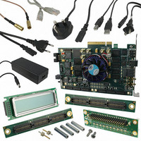
DK-DEV-4SGX230N Altera, DK-DEV-4SGX230N Datasheet - Page 137

DK-DEV-4SGX230N
Manufacturer Part Number
DK-DEV-4SGX230N
Description
KIT DEVELOPMENT STRATIX IV
Manufacturer
Altera
Series
Stratix® IVr
Type
FPGAr
Datasheets
1.EP4SGX110DF29C3N.pdf
(80 pages)
2.EP4SGX110DF29C3N.pdf
(1154 pages)
3.DK-DEV-4SGX230N.pdf
(2 pages)
4.DK-DEV-4SGX530N.pdf
(57 pages)
Specifications of DK-DEV-4SGX230N
Contents
Development Board, Universal Power Supply, Cables and Software
Silicon Manufacturer
Altera
Core Architecture
FPGA
Core Sub-architecture
Stratix
Silicon Core Number
EP4S
Silicon Family Name
Stratix IV GX
Rohs Compliant
Yes
For Use With/related Products
EP4SGX230K
Lead Free Status / RoHS Status
Lead free / RoHS Compliant
Other names
544-2594
Available stocks
Company
Part Number
Manufacturer
Quantity
Price
Company:
Part Number:
DK-DEV-4SGX230N
Manufacturer:
Altera
Quantity:
135
- EP4SGX110DF29C3N PDF datasheet
- EP4SGX110DF29C3N PDF datasheet #2
- DK-DEV-4SGX230N PDF datasheet #3
- DK-DEV-4SGX530N PDF datasheet #4
- Current page: 137 of 1154
- Download datasheet (32Mb)
Chapter 5: Clock Networks and PLLs in Stratix IV Devices
PLLs in Stratix IV Devices
Table 5–8. PLL Features in Stratix IV Devices (Part 2 of 2)
Figure 5–18. PLL Locations in Stratix IV Devices
February 2011 Altera Corporation
PLL cascading
Compensation modes
PLL drives LVDSCLK and LOADEN
VCO output drives the DPA clock
Phase shift resolution
Programmable duty cycle
Output counter cascading
Input clock switchover
Notes to
(1) While there is pin compatibility, there is no hard IP block placement compatibility.
(2) General purpose I/O pins cannot drive the PLL clock input pins.
(3) Provided input clock jitter is within input jitter tolerance specifications.
(4) The dedicated path between adjacent PLLs is not available on L1, L4, R1, and R4 PLLs.
(5) The smallest phase shift is determined by the voltage-controlled oscillator (VCO) period divided by eight. For degree increments, the Stratix IV
device can shift all output frequencies in increments of at least 45
divide parameters.
Left/Right PLLs
Left/Right PLLs
Table
5–8:
Feature
PLL_L1_CLK
PLL_L4_CLK
CLK[0..3]
Figure 5–18
L1
L2
L3
L4
shows the location of PLLs in Stratix IV devices.
Through GCLK and RCLK and a dedicated
Top/Bottom PLLs
Top/Bottom PLLs
All except LVDS clock network
Stratix IV Top/Bottom PLLs
path between adjacent PLLs
Down to 96.125 ps
compensation
CLK[12..15]
CLK[4..7]
Q1
Q4
B1 B2
T1
°
Yes
Yes
Yes
No
No
. Smaller degree increments are possible depending on the frequency and
(Note 1)
T2
Q2
Q3
Top/Bottom PLLs
Top/Bottom PLLs
(5)
dedicated path between adjacent PLLs
All except external feedback mode
Through GCLK and RCLK and
when using differential I/Os
R1
R2
R3
R4
Stratix IV Left/Right PLLs
Down to 96.125 ps
Stratix IV Device Handbook Volume 1
PLL_R1_CLK
CLK[8..11]
PLL-R4_CLK
Yes
Yes
Yes
Yes
Yes
(4)
Left/Right PLLs
Left/Right PLLs
(5)
5–21
Related parts for DK-DEV-4SGX230N
Image
Part Number
Description
Manufacturer
Datasheet
Request
R

Part Number:
Description:
KIT DEV ARRIA II GX FPGA 2AGX125
Manufacturer:
Altera
Datasheet:

Part Number:
Description:
KIT DEV CYCLONE III LS EP3CLS200
Manufacturer:
Altera
Datasheet:

Part Number:
Description:
KIT DEV STRATIX IV FPGA 4SE530
Manufacturer:
Altera
Datasheet:

Part Number:
Description:
KIT DEV FPGA 2AGX260 W/6.375G TX
Manufacturer:
Altera
Datasheet:

Part Number:
Description:
KIT DEV MAX V 5M570Z
Manufacturer:
Altera
Datasheet:

Part Number:
Description:
KIT DEV STRATIX V FPGA 5SGXEA7
Manufacturer:
Altera
Datasheet:

Part Number:
Description:
KIT DEVELOPMENT STRATIX III
Manufacturer:
Altera
Datasheet:

Part Number:
Description:
KIT DEV ARRIA GX 1AGX60N
Manufacturer:
Altera
Datasheet:

Part Number:
Description:
KIT STARTER CYCLONE IV GX
Manufacturer:
Altera
Datasheet:

Part Number:
Description:
KIT DEVELOPMENT STRATIX IV
Manufacturer:
Altera
Datasheet:

Part Number:
Description:
CPLD, EP610 Family, ECMOS Process, 300 Gates, 16 Macro Cells, 16 Reg., 16 User I/Os, 5V Supply, 35 Speed Grade, 24DIP
Manufacturer:
Altera Corporation
Datasheet:

Part Number:
Description:
CPLD, EP610 Family, ECMOS Process, 300 Gates, 16 Macro Cells, 16 Reg., 16 User I/Os, 5V Supply, 15 Speed Grade, 24DIP
Manufacturer:
Altera Corporation
Datasheet:


