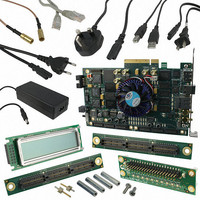
DK-DEV-4SGX230N Altera, DK-DEV-4SGX230N Datasheet - Page 138

DK-DEV-4SGX230N
Manufacturer Part Number
DK-DEV-4SGX230N
Description
KIT DEVELOPMENT STRATIX IV
Manufacturer
Altera
Series
Stratix® IVr
Type
FPGAr
Datasheets
1.EP4SGX110DF29C3N.pdf
(80 pages)
2.EP4SGX110DF29C3N.pdf
(1154 pages)
3.DK-DEV-4SGX230N.pdf
(2 pages)
4.DK-DEV-4SGX530N.pdf
(57 pages)
Specifications of DK-DEV-4SGX230N
Contents
Development Board, Universal Power Supply, Cables and Software
Silicon Manufacturer
Altera
Core Architecture
FPGA
Core Sub-architecture
Stratix
Silicon Core Number
EP4S
Silicon Family Name
Stratix IV GX
Rohs Compliant
Yes
For Use With/related Products
EP4SGX230K
Lead Free Status / RoHS Status
Lead free / RoHS Compliant
Other names
544-2594
Available stocks
Company
Part Number
Manufacturer
Quantity
Price
Company:
Part Number:
DK-DEV-4SGX230N
Manufacturer:
Altera
Quantity:
135
- EP4SGX110DF29C3N PDF datasheet
- EP4SGX110DF29C3N PDF datasheet #2
- DK-DEV-4SGX230N PDF datasheet #3
- DK-DEV-4SGX530N PDF datasheet #4
- Current page: 138 of 1154
- Download datasheet (32Mb)
5–22
Stratix IV Device Handbook Volume 1
Stratix IV PLL Hardware Overview
Stratix IV devices contain up to 12 PLLs with advanced clock management features.
The goal of a PLL is to synchronize the phase and frequency of an internal or external
clock to an input reference clock. There are a number of components that comprise a
PLL to achieve this phase alignment.
Stratix IV PLLs align the rising edge of the input reference clock to a feedback clock
using the phase-frequency detector (PFD). The falling edges are determined by the
duty-cycle specifications. The PFD produces an up or down signal that determines
whether the VCO must operate at a higher or lower frequency. The output of the PFD
feeds the charge pump and loop filter, which produces a control voltage for setting the
VCO frequency. If the PFD produces an up signal, the VCO frequency increases. A
down signal decreases the VCO frequency. The PFD outputs these up and down
signals to a charge pump. If the charge pump receives an up signal, current is driven
into the loop filter. Conversely, if the charge pump receives a down signal, current is
drawn from the loop filter.
The loop filter converts these up and down signals to a voltage that is used to bias the
VCO. The loop filter also removes glitches from the charge pump and prevents
voltage over-shoot, which filters the jitter on the VCO. The voltage from the loop filter
determines how fast the VCO operates. A divide counter (m) is inserted in the
feedback loop to increase the VCO frequency above the input reference frequency.
VCO frequency (f
reference clock (f
pre-scale counter (N). Therefore, the feedback clock (f
PFD is locked to the f
The VCO output from the left and right PLLs can feed seven post-scale counters
(C[0..6]), while the corresponding VCO output from the top and bottom PLLs can
feed ten post-scale counters (C[0..9]). These post-scale counters allow a number of
harmonically related frequencies to be produced by the PLL.
R EF
VCO
) to the PFD is equal to the input clock (f
) is equal to (m) times the input reference clock (f
REF
that is applied to the other input of the PFD.
Chapter 5: Clock Networks and PLLs in Stratix IV Devices
FB
) applied to one input of the
IN
February 2011 Altera Corporation
) divided by the
PLLs in Stratix IV Devices
R EF
). The input
Related parts for DK-DEV-4SGX230N
Image
Part Number
Description
Manufacturer
Datasheet
Request
R

Part Number:
Description:
KIT DEV ARRIA II GX FPGA 2AGX125
Manufacturer:
Altera
Datasheet:

Part Number:
Description:
KIT DEV CYCLONE III LS EP3CLS200
Manufacturer:
Altera
Datasheet:

Part Number:
Description:
KIT DEV STRATIX IV FPGA 4SE530
Manufacturer:
Altera
Datasheet:

Part Number:
Description:
KIT DEV FPGA 2AGX260 W/6.375G TX
Manufacturer:
Altera
Datasheet:

Part Number:
Description:
KIT DEV MAX V 5M570Z
Manufacturer:
Altera
Datasheet:

Part Number:
Description:
KIT DEV STRATIX V FPGA 5SGXEA7
Manufacturer:
Altera
Datasheet:

Part Number:
Description:
KIT DEVELOPMENT STRATIX III
Manufacturer:
Altera
Datasheet:

Part Number:
Description:
KIT DEV ARRIA GX 1AGX60N
Manufacturer:
Altera
Datasheet:

Part Number:
Description:
KIT STARTER CYCLONE IV GX
Manufacturer:
Altera
Datasheet:

Part Number:
Description:
KIT DEVELOPMENT STRATIX IV
Manufacturer:
Altera
Datasheet:

Part Number:
Description:
CPLD, EP610 Family, ECMOS Process, 300 Gates, 16 Macro Cells, 16 Reg., 16 User I/Os, 5V Supply, 35 Speed Grade, 24DIP
Manufacturer:
Altera Corporation
Datasheet:

Part Number:
Description:
CPLD, EP610 Family, ECMOS Process, 300 Gates, 16 Macro Cells, 16 Reg., 16 User I/Os, 5V Supply, 15 Speed Grade, 24DIP
Manufacturer:
Altera Corporation
Datasheet:


