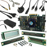
DK-DEV-4SGX230N Altera, DK-DEV-4SGX230N Datasheet - Page 331

DK-DEV-4SGX230N
Manufacturer Part Number
DK-DEV-4SGX230N
Description
KIT DEVELOPMENT STRATIX IV
Manufacturer
Altera
Series
Stratix® IVr
Type
FPGAr
Datasheets
1.EP4SGX110DF29C3N.pdf
(80 pages)
2.EP4SGX110DF29C3N.pdf
(1154 pages)
3.DK-DEV-4SGX230N.pdf
(2 pages)
4.DK-DEV-4SGX530N.pdf
(57 pages)
Specifications of DK-DEV-4SGX230N
Contents
Development Board, Universal Power Supply, Cables and Software
Silicon Manufacturer
Altera
Core Architecture
FPGA
Core Sub-architecture
Stratix
Silicon Core Number
EP4S
Silicon Family Name
Stratix IV GX
Rohs Compliant
Yes
For Use With/related Products
EP4SGX230K
Lead Free Status / RoHS Status
Lead free / RoHS Compliant
Other names
544-2594
Available stocks
Company
Part Number
Manufacturer
Quantity
Price
Company:
Part Number:
DK-DEV-4SGX230N
Manufacturer:
Altera
Quantity:
135
- EP4SGX110DF29C3N PDF datasheet
- EP4SGX110DF29C3N PDF datasheet #2
- DK-DEV-4SGX230N PDF datasheet #3
- DK-DEV-4SGX530N PDF datasheet #4
- Current page: 331 of 1154
- Download datasheet (32Mb)
Chapter 9: Hot Socketing and Power-On Reset in Stratix IV Devices
Hot-Socketing Feature Implementation in Stratix IV Devices
Hot-Socketing Feature Implementation in Stratix IV Devices
Figure 9–1. Hot-Socketing Circuitry for Stratix IV Devices
February 2011 Altera Corporation
1
The hot-socketing feature turns off the output buffer during power up and power
down of the V
circuitry generates an internal HOTSCKT signal when the V
or V
designed to prevent excess I/O leakage during power up. When the voltage ramps up
very slowly, it is still relatively low, even after the POR signal is released and the
configuration is completed. The CONF_DONE, nCEO, and nSTATUS pins fail to respond, as
the output buffer cannot flip from the state set by the hot-socketing circuit at this low
voltage. Therefore, the hot-socketing circuitry has been removed from these
configuration pins to make sure that they are able to operate during configuration.
Thus, it is expected behavior for these pins to drive out during power-up and
power-down sequences.
Figure 9–1
The POR circuit monitors the voltage level of the power supplies (V
V
The weak pull-up resistor (R) in the Stratix IV input/output element (IOE) keeps the
I/O pins from floating. The 3.0-V tolerance control circuit permits the I/O pins to be
driven by 3.0 V before the V
powered. It also prevents the I/O pins from driving out when the device is not in user
mode. To successfully power-up and exit POR on production devices, fully power
V
Altera uses GND as a reference for hot-socketing operations and I/O buffer designs.
To ensure proper operation, you must connect the GND between boards before
connecting the power supplies. This prevents the GND on your board from being
pulled up inadvertently by a path to power through other components on your board.
A pulled up GND could otherwise cause an out-of-specification I/O voltage or
current condition with the Altera device.
CCPGM
CC
Resistor
Pull-Up
Weak
CCPD
before V
PAD
, and V
power supplies are below the threshold voltage. Hot-socketing circuitry is
shows the Stratix IV device’s I/O pin circuitry.
R
CCAUX
CC
CCPD
, V
CCAUX
) and keeps the I/O pins tri-stated until the device is in user mode.
begins to ramp.
V
CCIO
, V
CCIO
CC
, V
, V
CCAUX
Tolerance
to Logic Array
CCPGM
Voltage
Control
Input Buffer
, V
, or V
CCPT
Output Enable
, V
CCPD
CCPGM
power supplies. The hot-socketing
Pre-Driver
Hot Socket
Output
Power On
, or V
Monitor
Reset
CC
Stratix IV Device Handbook Volume 1
, V
CCPD
CCAUX
supplies are
CC
, V
, V
CCIO
CCAUX
, V
CCPGM
, V
CCPT
9–3
,
,
Related parts for DK-DEV-4SGX230N
Image
Part Number
Description
Manufacturer
Datasheet
Request
R

Part Number:
Description:
KIT DEV ARRIA II GX FPGA 2AGX125
Manufacturer:
Altera
Datasheet:

Part Number:
Description:
KIT DEV CYCLONE III LS EP3CLS200
Manufacturer:
Altera
Datasheet:

Part Number:
Description:
KIT DEV STRATIX IV FPGA 4SE530
Manufacturer:
Altera
Datasheet:

Part Number:
Description:
KIT DEV FPGA 2AGX260 W/6.375G TX
Manufacturer:
Altera
Datasheet:

Part Number:
Description:
KIT DEV MAX V 5M570Z
Manufacturer:
Altera
Datasheet:

Part Number:
Description:
KIT DEV STRATIX V FPGA 5SGXEA7
Manufacturer:
Altera
Datasheet:

Part Number:
Description:
KIT DEVELOPMENT STRATIX III
Manufacturer:
Altera
Datasheet:

Part Number:
Description:
KIT DEV ARRIA GX 1AGX60N
Manufacturer:
Altera
Datasheet:

Part Number:
Description:
KIT STARTER CYCLONE IV GX
Manufacturer:
Altera
Datasheet:

Part Number:
Description:
KIT DEVELOPMENT STRATIX IV
Manufacturer:
Altera
Datasheet:

Part Number:
Description:
CPLD, EP610 Family, ECMOS Process, 300 Gates, 16 Macro Cells, 16 Reg., 16 User I/Os, 5V Supply, 35 Speed Grade, 24DIP
Manufacturer:
Altera Corporation
Datasheet:

Part Number:
Description:
CPLD, EP610 Family, ECMOS Process, 300 Gates, 16 Macro Cells, 16 Reg., 16 User I/Os, 5V Supply, 15 Speed Grade, 24DIP
Manufacturer:
Altera Corporation
Datasheet:


