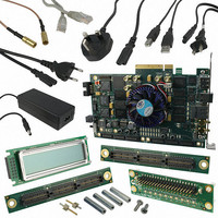
DK-DEV-4SGX230N Altera, DK-DEV-4SGX230N Datasheet - Page 734

DK-DEV-4SGX230N
Manufacturer Part Number
DK-DEV-4SGX230N
Description
KIT DEVELOPMENT STRATIX IV
Manufacturer
Altera
Series
Stratix® IVr
Type
FPGAr
Datasheets
1.EP4SGX110DF29C3N.pdf
(80 pages)
2.EP4SGX110DF29C3N.pdf
(1154 pages)
3.DK-DEV-4SGX230N.pdf
(2 pages)
4.DK-DEV-4SGX530N.pdf
(57 pages)
Specifications of DK-DEV-4SGX230N
Contents
Development Board, Universal Power Supply, Cables and Software
Silicon Manufacturer
Altera
Core Architecture
FPGA
Core Sub-architecture
Stratix
Silicon Core Number
EP4S
Silicon Family Name
Stratix IV GX
Rohs Compliant
Yes
For Use With/related Products
EP4SGX230K
Lead Free Status / RoHS Status
Lead free / RoHS Compliant
Other names
544-2594
Available stocks
Company
Part Number
Manufacturer
Quantity
Price
Company:
Part Number:
DK-DEV-4SGX230N
Manufacturer:
Altera
Quantity:
135
- EP4SGX110DF29C3N PDF datasheet
- EP4SGX110DF29C3N PDF datasheet #2
- DK-DEV-4SGX230N PDF datasheet #3
- DK-DEV-4SGX530N PDF datasheet #4
- Current page: 734 of 1154
- Download datasheet (32Mb)
2–62
Stratix IV Device Handbook Volume 2: Transceivers
1
Quartus II Software-Selected Receiver Phase Compensation FIFO Read Clock
If you do not select the rx_coreclk port in the ALTGX MegaWizard Plug-In Manager,
the Quartus II software automatically selects the receiver phase compensation FIFO
read clock for each channel in that ALTGX instance. The Quartus II software selects
the FIFO read clock depending on the channel configuration. In non-bonded channel
configurations, the FPGA fabric-receiver interface clocking has two scenarios:
■
■
Non-Bonded Channel Configuration with Rate Matcher
In non-bonded channel configuration, the transceiver channels may or may not be
identical. Identical transceiver channels are defined as channels that have exactly the
same CMU PLL and receiver CDR input reference clock sources, exactly the same
CMU PLL and receiver CDR configuration, and exactly the same PMA and PCS
configuration.
Example 6 assumes channels 0 and 1, driven by the CMU0 PLL in a transceiver block,
are identical. Also, channels 2 and 3, driven by the CMU1 PLL in the same transceiver
block, are identical. In this case, the Quartus II software automatically drives the read
port of the receiver phase compensation FIFO in channels 0 and 1 with the
tx_clkout[0] signal. It also drives the read port of the receiver phase compensation
FIFO in channels 2 and 3 with the tx_clkout[2] signal. Use the tx_clkout[0] signal
to latch the receiver data and status signals from channels 0 and 1 in the FPGA fabric.
Use the tx_clkout[2] signal to latch the receiver data and status signals from
channels 2 and 3 in the FPGA fabric.
This configuration uses two FPGA global and/or regional clock resources, one for the
tx_clkout[0] signal and the other for the tx_clkout[2] signal.
Receivers that do not use a rate matcher block (refer to
Clocking Without Rate Matcher” on page
Receivers that use a rate matcher block (refer to
with Rate Matcher” on page
Example 6: Two Groups of Two Identical Channels in a Transceiver Block
2–41)
2–39)
Chapter 2: Transceiver Clocking in Stratix IV Devices
“Non-Bonded Receiver Clocking
FPGA Fabric-Transceiver Interface Clocking
“Non-Bonded Receiver
February 2011 Altera Corporation
Related parts for DK-DEV-4SGX230N
Image
Part Number
Description
Manufacturer
Datasheet
Request
R

Part Number:
Description:
KIT DEV ARRIA II GX FPGA 2AGX125
Manufacturer:
Altera
Datasheet:

Part Number:
Description:
KIT DEV CYCLONE III LS EP3CLS200
Manufacturer:
Altera
Datasheet:

Part Number:
Description:
KIT DEV STRATIX IV FPGA 4SE530
Manufacturer:
Altera
Datasheet:

Part Number:
Description:
KIT DEV FPGA 2AGX260 W/6.375G TX
Manufacturer:
Altera
Datasheet:

Part Number:
Description:
KIT DEV MAX V 5M570Z
Manufacturer:
Altera
Datasheet:

Part Number:
Description:
KIT DEV STRATIX V FPGA 5SGXEA7
Manufacturer:
Altera
Datasheet:

Part Number:
Description:
KIT DEVELOPMENT STRATIX III
Manufacturer:
Altera
Datasheet:

Part Number:
Description:
KIT DEV ARRIA GX 1AGX60N
Manufacturer:
Altera
Datasheet:

Part Number:
Description:
KIT STARTER CYCLONE IV GX
Manufacturer:
Altera
Datasheet:

Part Number:
Description:
KIT DEVELOPMENT STRATIX IV
Manufacturer:
Altera
Datasheet:

Part Number:
Description:
CPLD, EP610 Family, ECMOS Process, 300 Gates, 16 Macro Cells, 16 Reg., 16 User I/Os, 5V Supply, 35 Speed Grade, 24DIP
Manufacturer:
Altera Corporation
Datasheet:

Part Number:
Description:
CPLD, EP610 Family, ECMOS Process, 300 Gates, 16 Macro Cells, 16 Reg., 16 User I/Os, 5V Supply, 15 Speed Grade, 24DIP
Manufacturer:
Altera Corporation
Datasheet:


