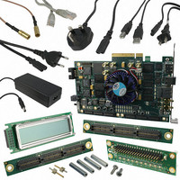
DK-DEV-4SGX230N Altera, DK-DEV-4SGX230N Datasheet - Page 304

DK-DEV-4SGX230N
Manufacturer Part Number
DK-DEV-4SGX230N
Description
KIT DEVELOPMENT STRATIX IV
Manufacturer
Altera
Series
Stratix® IVr
Type
FPGAr
Datasheets
1.EP4SGX110DF29C3N.pdf
(80 pages)
2.EP4SGX110DF29C3N.pdf
(1154 pages)
3.DK-DEV-4SGX230N.pdf
(2 pages)
4.DK-DEV-4SGX530N.pdf
(57 pages)
Specifications of DK-DEV-4SGX230N
Contents
Development Board, Universal Power Supply, Cables and Software
Silicon Manufacturer
Altera
Core Architecture
FPGA
Core Sub-architecture
Stratix
Silicon Core Number
EP4S
Silicon Family Name
Stratix IV GX
Rohs Compliant
Yes
For Use With/related Products
EP4SGX230K
Lead Free Status / RoHS Status
Lead free / RoHS Compliant
Other names
544-2594
Available stocks
Company
Part Number
Manufacturer
Quantity
Price
Company:
Part Number:
DK-DEV-4SGX230N
Manufacturer:
Altera
Quantity:
135
- EP4SGX110DF29C3N PDF datasheet
- EP4SGX110DF29C3N PDF datasheet #2
- DK-DEV-4SGX230N PDF datasheet #3
- DK-DEV-4SGX530N PDF datasheet #4
- Current page: 304 of 1154
- Download datasheet (32Mb)
8–26
LVDS Interface with the Use External PLL Option Enabled
Table 8–10. Signal Interface Between ALTPLL and ALTLVDS Megafunctions (Part 1 of 2)
Stratix IV Device Handbook Volume 1
Serial clock output (c0)
Load enable output (c1)
From the ALTPLL
Megafunction
f
1
1
You can use every LVDS channel in soft-CDR mode and can drive the FPGA fabric
using the periphery clock network in the Stratix IV device family. The rx_dpa_locked
signal is not valid in soft-CDR mode because the DPA continuously changes its phase
to track PPM differences between the upstream transmitter and the local receiver
input reference clocks. The parallel clock rx_outclock, generated by the left and right
PLL, is also forwarded to the FPGA fabric.
The ALTLVDS MegaWizard Plug-In Manager software provides an option for
implementing the LVDS interface with the Use External PLL option. With this option
enabled you can control the PLL settings, such as dynamically reconfiguring the PLL
to support different data rates, dynamic phase shift, and other settings. You also must
instantiate an ALTPLL megafunction to generate the various clock and load enable
signals.
When you enable the Use External PLL option with the ALTLVDS transmitter and
receiver, the following signals are required from the ALTPLL megafunction:
■
■
■
■
As an example,
parallel clock output generated on ports c0, c1, and c2, respectively, along with the
locked signal of the ALTPLL instance. You can choose any of the PLL output clock
ports to generate the interface clocks.
With soft SERDES, a different clocking requirement is needed. For more information,
refer to the
Guide.
The high-speed clock generated from the PLL is intended to clock the LVDS SERDES
circuitry only. Do not use the high-speed clock to drive other logic because the
allowed frequency to drive the core logic is restricted by the PLL F
For more information about the F
Characteristics for Stratix IV Devices
Table 8–10
megafunction and the input ports of the ALTLVDS transmitter and receiver.
(1)
Serial clock input to the SERDES of the ALTLVDS transmitter and receiver
Load enable to the SERDES of the ALTLVDS transmitter and receiver
Parallel clock used to clock the transmitter FPGA fabric logic and parallel clock
used for the receiver rx_syncclock port and receiver FPGA fabric logic
Asynchronous PLL reset port of the ALTLVDS receiver
tx_inclock (serial clock input to the
transmitter)
tx_enable (load enable to the transmitter)
lists the signal interface between the output ports of the ALTPLL
LVDS SERDES Transmitter/Receiver (ALTLVDS_RX/TX) Megafunction User
Table 8–10
To the ALTLVDS Transmitter
Chapter 8: High-Speed Differential I/O Interfaces and DPA in Stratix IV Devices
describes the serial clock output, load enable output, and
OUT
chapter.
specification, refer to the
LVDS Interface with the Use External PLL Option Enabled
rx_inclock (serial clock input)
rx_enable (load enable for the
deserializer)
To the ALTLVDS Receiver
February 2011 Altera Corporation
DC and Switching
OUT
specification.
Related parts for DK-DEV-4SGX230N
Image
Part Number
Description
Manufacturer
Datasheet
Request
R

Part Number:
Description:
KIT DEV ARRIA II GX FPGA 2AGX125
Manufacturer:
Altera
Datasheet:

Part Number:
Description:
KIT DEV CYCLONE III LS EP3CLS200
Manufacturer:
Altera
Datasheet:

Part Number:
Description:
KIT DEV STRATIX IV FPGA 4SE530
Manufacturer:
Altera
Datasheet:

Part Number:
Description:
KIT DEV FPGA 2AGX260 W/6.375G TX
Manufacturer:
Altera
Datasheet:

Part Number:
Description:
KIT DEV MAX V 5M570Z
Manufacturer:
Altera
Datasheet:

Part Number:
Description:
KIT DEV STRATIX V FPGA 5SGXEA7
Manufacturer:
Altera
Datasheet:

Part Number:
Description:
KIT DEVELOPMENT STRATIX III
Manufacturer:
Altera
Datasheet:

Part Number:
Description:
KIT DEV ARRIA GX 1AGX60N
Manufacturer:
Altera
Datasheet:

Part Number:
Description:
KIT STARTER CYCLONE IV GX
Manufacturer:
Altera
Datasheet:

Part Number:
Description:
KIT DEVELOPMENT STRATIX IV
Manufacturer:
Altera
Datasheet:

Part Number:
Description:
CPLD, EP610 Family, ECMOS Process, 300 Gates, 16 Macro Cells, 16 Reg., 16 User I/Os, 5V Supply, 35 Speed Grade, 24DIP
Manufacturer:
Altera Corporation
Datasheet:

Part Number:
Description:
CPLD, EP610 Family, ECMOS Process, 300 Gates, 16 Macro Cells, 16 Reg., 16 User I/Os, 5V Supply, 15 Speed Grade, 24DIP
Manufacturer:
Altera Corporation
Datasheet:


