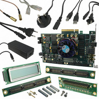
DK-DEV-4SGX230N Altera, DK-DEV-4SGX230N Datasheet - Page 155

DK-DEV-4SGX230N
Manufacturer Part Number
DK-DEV-4SGX230N
Description
KIT DEVELOPMENT STRATIX IV
Manufacturer
Altera
Series
Stratix® IVr
Type
FPGAr
Datasheets
1.EP4SGX110DF29C3N.pdf
(80 pages)
2.EP4SGX110DF29C3N.pdf
(1154 pages)
3.DK-DEV-4SGX230N.pdf
(2 pages)
4.DK-DEV-4SGX530N.pdf
(57 pages)
Specifications of DK-DEV-4SGX230N
Contents
Development Board, Universal Power Supply, Cables and Software
Silicon Manufacturer
Altera
Core Architecture
FPGA
Core Sub-architecture
Stratix
Silicon Core Number
EP4S
Silicon Family Name
Stratix IV GX
Rohs Compliant
Yes
For Use With/related Products
EP4SGX230K
Lead Free Status / RoHS Status
Lead free / RoHS Compliant
Other names
544-2594
Available stocks
Company
Part Number
Manufacturer
Quantity
Price
Company:
Part Number:
DK-DEV-4SGX230N
Manufacturer:
Altera
Quantity:
135
- EP4SGX110DF29C3N PDF datasheet
- EP4SGX110DF29C3N PDF datasheet #2
- DK-DEV-4SGX230N PDF datasheet #3
- DK-DEV-4SGX530N PDF datasheet #4
- Current page: 155 of 1154
- Download datasheet (32Mb)
Chapter 5: Clock Networks and PLLs in Stratix IV Devices
PLLs in Stratix IV Devices
Figure 5–34. Automatic Clock Switchover Circuit Block Diagram
February 2011 Altera Corporation
1
inclk0
inclk1
Stratix IV PLLs support a fully configurable clock switchover capability.
shows a block diagram of the automatic switchover circuit built into the PLL. When
the current reference clock is not present, the clock sense block automatically switches
to the backup clock for PLL reference. The clock switchover circuit also sends out
three status signals—clkbad[0], clkbad[1], and activeclock—from the PLL to
implement a custom switchover circuit in the logic array. You can select a clock source
as the backup clock by connecting it to the inclk1 port of the PLL in your design.
Automatic Clock Switchover
Use the switchover circuitry to automatically switch between inclk0 and inclk1
when the current reference clock to the PLL stops toggling. For example, in
applications that require a redundant clock with the same frequency as the reference
clock, the switchover state machine generates a signal (clksw) that controls the
multiplexer select input, as shown in
reference clock for the PLL. When using automatic switchover mode, you can switch
back and forth between inclk0 and inclk1 any number of times when one of the two
clocks fails and the other clock is available.
When using automatic clock switchover mode, the following requirements must be
satisfied:
■
■
If the current clock input stops toggling while the other clock is also not toggling,
switchover is not initiated and the clkbad[0..1] signals are not valid. Also, if both
clock inputs are not the same frequency, but their period difference is within 100%, the
clock sense block detects when a clock stops toggling, but the PLL may lose lock after
the switchover is completed and needs time to re-lock.
Altera recommends resetting the PLL using the areset signal to maintain the phase
relationships between the PLL input and output clocks when using clock switchover.
Both clock inputs must be running
The period of the two clock inputs can differ by no more than 100% (2×)
muxout
clksw
n Counter
Sense
Clock
refclk
Figure
Switchover
Machine
State
5–34. In this case, inclk1 becomes the
Clock Switch
Control Logic
PFD
fbclk
Stratix IV Device Handbook Volume 1
clkbad[0]
clkbad[1]
activeclock
clkswitch
Figure 5–34
5–39
Related parts for DK-DEV-4SGX230N
Image
Part Number
Description
Manufacturer
Datasheet
Request
R

Part Number:
Description:
KIT DEV ARRIA II GX FPGA 2AGX125
Manufacturer:
Altera
Datasheet:

Part Number:
Description:
KIT DEV CYCLONE III LS EP3CLS200
Manufacturer:
Altera
Datasheet:

Part Number:
Description:
KIT DEV STRATIX IV FPGA 4SE530
Manufacturer:
Altera
Datasheet:

Part Number:
Description:
KIT DEV FPGA 2AGX260 W/6.375G TX
Manufacturer:
Altera
Datasheet:

Part Number:
Description:
KIT DEV MAX V 5M570Z
Manufacturer:
Altera
Datasheet:

Part Number:
Description:
KIT DEV STRATIX V FPGA 5SGXEA7
Manufacturer:
Altera
Datasheet:

Part Number:
Description:
KIT DEVELOPMENT STRATIX III
Manufacturer:
Altera
Datasheet:

Part Number:
Description:
KIT DEV ARRIA GX 1AGX60N
Manufacturer:
Altera
Datasheet:

Part Number:
Description:
KIT STARTER CYCLONE IV GX
Manufacturer:
Altera
Datasheet:

Part Number:
Description:
KIT DEVELOPMENT STRATIX IV
Manufacturer:
Altera
Datasheet:

Part Number:
Description:
CPLD, EP610 Family, ECMOS Process, 300 Gates, 16 Macro Cells, 16 Reg., 16 User I/Os, 5V Supply, 35 Speed Grade, 24DIP
Manufacturer:
Altera Corporation
Datasheet:

Part Number:
Description:
CPLD, EP610 Family, ECMOS Process, 300 Gates, 16 Macro Cells, 16 Reg., 16 User I/Os, 5V Supply, 15 Speed Grade, 24DIP
Manufacturer:
Altera Corporation
Datasheet:


