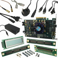
DK-DEV-4SGX230N Altera, DK-DEV-4SGX230N Datasheet - Page 40

DK-DEV-4SGX230N
Manufacturer Part Number
DK-DEV-4SGX230N
Description
KIT DEVELOPMENT STRATIX IV
Manufacturer
Altera
Series
Stratix® IVr
Type
FPGAr
Datasheets
1.EP4SGX110DF29C3N.pdf
(80 pages)
2.EP4SGX110DF29C3N.pdf
(1154 pages)
3.DK-DEV-4SGX230N.pdf
(2 pages)
4.DK-DEV-4SGX530N.pdf
(57 pages)
Specifications of DK-DEV-4SGX230N
Contents
Development Board, Universal Power Supply, Cables and Software
Silicon Manufacturer
Altera
Core Architecture
FPGA
Core Sub-architecture
Stratix
Silicon Core Number
EP4S
Silicon Family Name
Stratix IV GX
Rohs Compliant
Yes
For Use With/related Products
EP4SGX230K
Lead Free Status / RoHS Status
Lead free / RoHS Compliant
Other names
544-2594
Available stocks
Company
Part Number
Manufacturer
Quantity
Price
Company:
Part Number:
DK-DEV-4SGX230N
Manufacturer:
Altera
Quantity:
135
- EP4SGX110DF29C3N PDF datasheet
- EP4SGX110DF29C3N PDF datasheet #2
- DK-DEV-4SGX230N PDF datasheet #3
- DK-DEV-4SGX530N PDF datasheet #4
- Current page: 40 of 1154
- Download datasheet (32Mb)
2–4
Figure 2–3. Direct-Link Connection
Stratix IV Device Handbook Volume 1
Direct-link
interconnect
to left
LAB Interconnects
LAB Control Signals
Direct-link interconnect from the
block, DSP block, or IOE output
ALMs
left LAB, TriMatrix memory
The LAB local interconnect can drive ALMs in the same LAB. It is driven by column
and row interconnects and ALM outputs in the same LAB. Neighboring
LABs/MLABs, M9K RAM blocks, M144K blocks, or digital signal processing (DSP)
blocks from the left or right can also drive the LAB’s local interconnect through the
direct link connection. The direct link connection feature minimizes the use of row
and column interconnects, providing higher performance and flexibility. Each LAB
can drive 30 ALMs through fast-local and direct-link interconnects.
Figure 2–3
Each LAB contains dedicated logic for driving control signals to its ALMs. Control
signals include three clocks, three clock enables, two asynchronous clears, a
synchronous clear, and synchronous load control signals. This gives a maximum of 10
control signals at a time. Although you generally use synchronous-load and clear
signals when implementing counters, you can also use them with other functions.
Each LAB has two unique clock sources and three clock enable signals, as shown in
Figure
sources and three clock enable signals. Each LAB’s clock and clock enable signals are
linked. For example, any ALM in a particular LAB using the labclk1 signal also uses
the labclkena1 signal. If the LAB uses both the rising and falling edges of a clock, it
also uses two LAB-wide clock signals. De-asserting the clock enable signal turns off
the corresponding LAB-wide clock.
2–4. The LAB control block can generate up to three clocks using two clock
MLAB
shows the direct-link connection.
Interconnect
Local
Chapter 2: Logic Array Blocks and Adaptive Logic Modules in Stratix IV Devices
LAB
ALMs
Direct-link
interconnect
to right
Direct-link interconnect from the
right LAB, TriMatrix memory
block, DSP block, or IOE output
February 2011 Altera Corporation
Logic Array Blocks
Related parts for DK-DEV-4SGX230N
Image
Part Number
Description
Manufacturer
Datasheet
Request
R

Part Number:
Description:
KIT DEV ARRIA II GX FPGA 2AGX125
Manufacturer:
Altera
Datasheet:

Part Number:
Description:
KIT DEV CYCLONE III LS EP3CLS200
Manufacturer:
Altera
Datasheet:

Part Number:
Description:
KIT DEV STRATIX IV FPGA 4SE530
Manufacturer:
Altera
Datasheet:

Part Number:
Description:
KIT DEV FPGA 2AGX260 W/6.375G TX
Manufacturer:
Altera
Datasheet:

Part Number:
Description:
KIT DEV MAX V 5M570Z
Manufacturer:
Altera
Datasheet:

Part Number:
Description:
KIT DEV STRATIX V FPGA 5SGXEA7
Manufacturer:
Altera
Datasheet:

Part Number:
Description:
KIT DEVELOPMENT STRATIX III
Manufacturer:
Altera
Datasheet:

Part Number:
Description:
KIT DEV ARRIA GX 1AGX60N
Manufacturer:
Altera
Datasheet:

Part Number:
Description:
KIT STARTER CYCLONE IV GX
Manufacturer:
Altera
Datasheet:

Part Number:
Description:
KIT DEVELOPMENT STRATIX IV
Manufacturer:
Altera
Datasheet:

Part Number:
Description:
CPLD, EP610 Family, ECMOS Process, 300 Gates, 16 Macro Cells, 16 Reg., 16 User I/Os, 5V Supply, 35 Speed Grade, 24DIP
Manufacturer:
Altera Corporation
Datasheet:

Part Number:
Description:
CPLD, EP610 Family, ECMOS Process, 300 Gates, 16 Macro Cells, 16 Reg., 16 User I/Os, 5V Supply, 15 Speed Grade, 24DIP
Manufacturer:
Altera Corporation
Datasheet:


