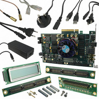
DK-DEV-4SGX230N Altera, DK-DEV-4SGX230N Datasheet - Page 289

DK-DEV-4SGX230N
Manufacturer Part Number
DK-DEV-4SGX230N
Description
KIT DEVELOPMENT STRATIX IV
Manufacturer
Altera
Series
Stratix® IVr
Type
FPGAr
Datasheets
1.EP4SGX110DF29C3N.pdf
(80 pages)
2.EP4SGX110DF29C3N.pdf
(1154 pages)
3.DK-DEV-4SGX230N.pdf
(2 pages)
4.DK-DEV-4SGX530N.pdf
(57 pages)
Specifications of DK-DEV-4SGX230N
Contents
Development Board, Universal Power Supply, Cables and Software
Silicon Manufacturer
Altera
Core Architecture
FPGA
Core Sub-architecture
Stratix
Silicon Core Number
EP4S
Silicon Family Name
Stratix IV GX
Rohs Compliant
Yes
For Use With/related Products
EP4SGX230K
Lead Free Status / RoHS Status
Lead free / RoHS Compliant
Other names
544-2594
Available stocks
Company
Part Number
Manufacturer
Quantity
Price
Company:
Part Number:
DK-DEV-4SGX230N
Manufacturer:
Altera
Quantity:
135
- EP4SGX110DF29C3N PDF datasheet
- EP4SGX110DF29C3N PDF datasheet #2
- DK-DEV-4SGX230N PDF datasheet #3
- DK-DEV-4SGX530N PDF datasheet #4
- Current page: 289 of 1154
- Download datasheet (32Mb)
Chapter 8: High-Speed Differential I/O Interfaces and DPA in Stratix IV Devices
Differential Transmitter
Table 8–7. Port List of the LVDS Interface (ALTLVDS)
Differential Transmitter
February 2011 Altera Corporation
dpa_pll_cal_busy
rx_reset
rx_fifo_reset
rx_cda_reset
Notes to
(1) Unless stated, signals are valid in all three modes (non-DPA, DPA, and soft-CDR) for a single channel.
(2) All reset and control signals are active high.
(3) For more information, refer to
Reset Signals
Table
Port Name
8–7:
f
1
For more information about the LVDS transmitter and receiver settings using
ALTLVDS, refer to the
The Stratix IV transmitter has a dedicated circuitry to provide support for LVDS
signaling. The dedicated circuitry consists of a differential buffer, a serializer, and left
and right PLLs that can be shared between the transmitter and receiver. The
differential buffer can drive out LVDS, mini-LVDS, and RSDS signaling levels. The
serializer takes up to 10 bits wide parallel data from the FPGA fabric, clocks it into the
load registers, and serializes it using shift registers clocked by the left and right PLL
before sending the data to the differential buffer. The MSB of the parallel data is
transmitted first.
When using emulated LVDS I/O standards at the differential transmitter, the
SERDES circuitry must be implemented in logic cells but not hard SERDES.
“LVDS Interface with the Use External PLL Option Enabled” on page
Output
Input
Input
Input
Output
Input /
Busy signal that is asserted high when the PLL calibration occurs.
Asynchronous reset to the DPA circuitry and FIFO. The minimum pulse
width requirement for this reset is one parallel clock cycle. This signal
resets DPA and FIFO blocks.
Asynchronous reset to the FIFO between the DPA and the data realignment
circuits. The synchronizer block must be reset after a DPA loses lock
condition and the data checker shows corrupted received data. The
minimum pulse width requirement for this reset is one parallel clock cycle.
This signal resets the FIFO block.
Asynchronous reset to the data realignment circuitry. The minimum pulse
width requirement for this reset is one parallel clock cycle. This signal
resets the data realignment block.
ALTLVDS Megafunction User
(Note
1),
(2)
(Part 3 of 3)
Description
Guide.
8–26.
Stratix IV Device Handbook Volume 1
8–11
Related parts for DK-DEV-4SGX230N
Image
Part Number
Description
Manufacturer
Datasheet
Request
R

Part Number:
Description:
KIT DEV ARRIA II GX FPGA 2AGX125
Manufacturer:
Altera
Datasheet:

Part Number:
Description:
KIT DEV CYCLONE III LS EP3CLS200
Manufacturer:
Altera
Datasheet:

Part Number:
Description:
KIT DEV STRATIX IV FPGA 4SE530
Manufacturer:
Altera
Datasheet:

Part Number:
Description:
KIT DEV FPGA 2AGX260 W/6.375G TX
Manufacturer:
Altera
Datasheet:

Part Number:
Description:
KIT DEV MAX V 5M570Z
Manufacturer:
Altera
Datasheet:

Part Number:
Description:
KIT DEV STRATIX V FPGA 5SGXEA7
Manufacturer:
Altera
Datasheet:

Part Number:
Description:
KIT DEVELOPMENT STRATIX III
Manufacturer:
Altera
Datasheet:

Part Number:
Description:
KIT DEV ARRIA GX 1AGX60N
Manufacturer:
Altera
Datasheet:

Part Number:
Description:
KIT STARTER CYCLONE IV GX
Manufacturer:
Altera
Datasheet:

Part Number:
Description:
KIT DEVELOPMENT STRATIX IV
Manufacturer:
Altera
Datasheet:

Part Number:
Description:
CPLD, EP610 Family, ECMOS Process, 300 Gates, 16 Macro Cells, 16 Reg., 16 User I/Os, 5V Supply, 35 Speed Grade, 24DIP
Manufacturer:
Altera Corporation
Datasheet:

Part Number:
Description:
CPLD, EP610 Family, ECMOS Process, 300 Gates, 16 Macro Cells, 16 Reg., 16 User I/Os, 5V Supply, 15 Speed Grade, 24DIP
Manufacturer:
Altera Corporation
Datasheet:


