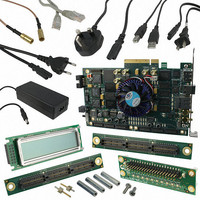
DK-DEV-4SGX230N Altera, DK-DEV-4SGX230N Datasheet - Page 59

DK-DEV-4SGX230N
Manufacturer Part Number
DK-DEV-4SGX230N
Description
KIT DEVELOPMENT STRATIX IV
Manufacturer
Altera
Series
Stratix® IVr
Type
FPGAr
Datasheets
1.EP4SGX110DF29C3N.pdf
(80 pages)
2.EP4SGX110DF29C3N.pdf
(1154 pages)
3.DK-DEV-4SGX230N.pdf
(2 pages)
4.DK-DEV-4SGX530N.pdf
(57 pages)
Specifications of DK-DEV-4SGX230N
Contents
Development Board, Universal Power Supply, Cables and Software
Silicon Manufacturer
Altera
Core Architecture
FPGA
Core Sub-architecture
Stratix
Silicon Core Number
EP4S
Silicon Family Name
Stratix IV GX
Rohs Compliant
Yes
For Use With/related Products
EP4SGX230K
Lead Free Status / RoHS Status
Lead free / RoHS Compliant
Other names
544-2594
Available stocks
Company
Part Number
Manufacturer
Quantity
Price
Company:
Part Number:
DK-DEV-4SGX230N
Manufacturer:
Altera
Quantity:
135
- EP4SGX110DF29C3N PDF datasheet
- EP4SGX110DF29C3N PDF datasheet #2
- DK-DEV-4SGX230N PDF datasheet #3
- DK-DEV-4SGX530N PDF datasheet #4
- Current page: 59 of 1154
- Download datasheet (32Mb)
Chapter 3: TriMatrix Embedded Memory Blocks in Stratix IV Devices
Overview
Table 3–2. TriMatrix Memory Capacity and Distribution in Stratix IV Devices (Part 2 of 2)
February 2011 Altera Corporation
EP4SGX180
EP4SGX230
EP4SGX290
EP4SGX360
EP4SGX530
EP4S40G2
EP4S40G5
EP4S100G2
EP4S100G3
EP4S100G4
EP4S100G5
Device
TriMatrix Memory Block Types
Parity Bit Support
Byte Enable Support
While the M9K and M144K memory blocks are dedicated resources, the MLABs are
dual-purpose blocks. They can be configured as regular logic array blocks (LABs) or
as MLABs. Ten adaptive logic modules (ALMs) make up one MLAB. You can
configure each ALM in an MLAB as either a 64 × 1 or a 32 × 2 block, resulting in a
64 × 10 or 32 × 20 simple dual-port SRAM block in a single MLAB.
All TriMatrix memory blocks have built-in parity-bit support. The ninth bit associated
with each byte can store a parity bit or serve as an additional data bit. No parity
function is actually performed on the ninth bit.
All TriMatrix memory blocks support byte enables that mask the input data so that
only specific bytes of data are written. The unwritten bytes retain the previously
written values. The write enable (wren) signals, along with the byte enable (byteena)
signals, control the RAM blocks’ write operations.
The default value for the byte enable signals is high (enabled), in which case writing is
controlled only by the write enable signals. The byte enable registers have no clear
port. When using parity bits on the M9K and M144K blocks, the byte enable controls
all nine bits (eight bits of data plus one parity bit). When using parity bits on the
MLAB, the byte-enable controls all 10 bits in the widest mode.
The MSB for the byteena signal corresponds to the MSB of the data bus and the LSB of
the byteena signal corresponds to the LSB of the data bus. For example, if you use a
RAM block in ×18 mode, with byteena = 01, data[8..0] is enabled, and data[17..9]
id disabled. Similarly, if byteena = 11, both data[8..0] and data[17..9] are enabled.
Byte enables are active high.
MLABs
10,624
10,624
10,624
3,515
4,560
5,824
7,072
4,560
4,560
5,824
7,072
M9K Blocks
1,235
1,248
1,280
1,235
1,235
1,248
1,280
1280
950
936
936
M144K
Blocks
20
22
36
48
64
22
64
22
36
48
64
(Dedicated Memory Blocks Only)
Total Dedicated RAM Bits
11,430
14,283
13,608
18,144
20,736
14,283
20,736
14,283
13,608
18,144
20,736
(Kb)
Stratix IV Device Handbook Volume 1
(Including MLABs)
Total RAM Bits
13,627
17,133
17,248
22,564
27,376
17,133
27,376
17,133
17,248
22,564
27,376
(Kb)
3–3
Related parts for DK-DEV-4SGX230N
Image
Part Number
Description
Manufacturer
Datasheet
Request
R

Part Number:
Description:
KIT DEV ARRIA II GX FPGA 2AGX125
Manufacturer:
Altera
Datasheet:

Part Number:
Description:
KIT DEV CYCLONE III LS EP3CLS200
Manufacturer:
Altera
Datasheet:

Part Number:
Description:
KIT DEV STRATIX IV FPGA 4SE530
Manufacturer:
Altera
Datasheet:

Part Number:
Description:
KIT DEV FPGA 2AGX260 W/6.375G TX
Manufacturer:
Altera
Datasheet:

Part Number:
Description:
KIT DEV MAX V 5M570Z
Manufacturer:
Altera
Datasheet:

Part Number:
Description:
KIT DEV STRATIX V FPGA 5SGXEA7
Manufacturer:
Altera
Datasheet:

Part Number:
Description:
KIT DEVELOPMENT STRATIX III
Manufacturer:
Altera
Datasheet:

Part Number:
Description:
KIT DEV ARRIA GX 1AGX60N
Manufacturer:
Altera
Datasheet:

Part Number:
Description:
KIT STARTER CYCLONE IV GX
Manufacturer:
Altera
Datasheet:

Part Number:
Description:
KIT DEVELOPMENT STRATIX IV
Manufacturer:
Altera
Datasheet:

Part Number:
Description:
CPLD, EP610 Family, ECMOS Process, 300 Gates, 16 Macro Cells, 16 Reg., 16 User I/Os, 5V Supply, 35 Speed Grade, 24DIP
Manufacturer:
Altera Corporation
Datasheet:

Part Number:
Description:
CPLD, EP610 Family, ECMOS Process, 300 Gates, 16 Macro Cells, 16 Reg., 16 User I/Os, 5V Supply, 15 Speed Grade, 24DIP
Manufacturer:
Altera Corporation
Datasheet:


